Signal Descriptions
Copyright © ARM Limited 2000. All rights reserved.
B-3
B.2
Clock interface signals
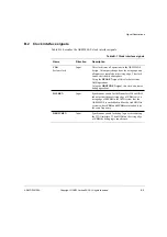
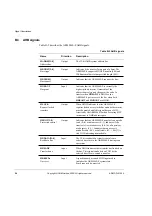
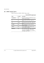
Table B-1 describes the ARM946E-S clock interface signals.
Table B-1 Clock interface signals
Name
Direction
Description
CLK
System clock
Input
This clock times all operations in the ARM946E-S
design. All outputs change from the rising edge and
all inputs are sampled on the rising edge. The clock
can be stretched in either phase.
Using the HCLKEN signal, this clock also times
AHB operations.
Using the DBGTCKEN signal, this clock also times
debug operations.
HCLKEN
Input
Synchronous enable for AHB transfers. When HIGH
indicates that the next rising edge of CLK is also a
rising edge of HCLK in the AHB system that the
ARM946E-S is embedded in. Must be tied HIGH in
systems where CLK and HCLK are intended to be
the same frequency.
DBGTCKEN
Input
Synchronous enable for debug logic accessed using
the JTAG interface. When HIGH on the rising edge
of CLK the debug logic can advance.
Содержание ARM946E-S
Страница 1: ...ARM DDI 0155A ARM946E S Technical Reference Manual ...
Страница 6: ...vi Copyright ARM Limited 2000 All rights reserved ARM DDI 0155A 04 Limited Confidential ...
Страница 54: ...Programmer s Model 2 34 Copyright ARM Limited 2000 All rights reserved ARM DDI 0155A ...
Страница 70: ...Caches 3 16 Copyright ARM Limited 2000 All rights reserved ARM DDI 0155A ...
Страница 78: ...Protection Unit 4 8 Copyright ARM Limited 2000 All rights reserved ARM DDI 0155A ...
Страница 98: ...Bus Interface Unit and Write Buffer 6 14 Copyright ARM Limited 2000 All rights reserved ARM DDI 0155A ...
Страница 112: ...Coprocessor Interface 7 14 Copyright ARM Limited 2000 All rights reserved ARM DDI 0155A ...

