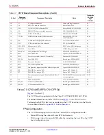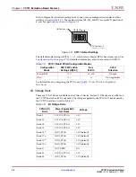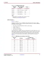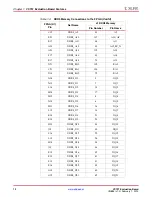
VC707 Evaluation Board
19
UG885 (v1.2) February 1, 2013
Feature Descriptions
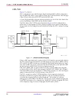
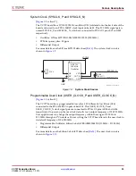
The USB3320 is clocked by a 24 MHz crystal. The ULPI interface supports two clocking
modes selected by jumper on J14:
•
24 MHz ULPI output clock mode (default): No jumper on J14. The PHY drives the
UPLI clock. This is the default setting.
•
60 MHz ULPI input clock mode: Jumper across J14 pins 1–2.
Consult the SMSC USB3320 data sheet for clocking mode details
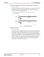
The FPGA interface to the USB3320 transceiver is implemented through the AXI universal
serial bus 2.0 device IP. See
LogiCORE IP AXI Universal Serial Bus 2.0 Device
.
Note:
The AXI universal serial bus 2.0 device IP supports USB-supplied power mode only. Jumpers
on headers J13 and J45 must be configured to their default state as described here:
•
J13 = jumper removed
•
J45 = jumper across pins 1–2
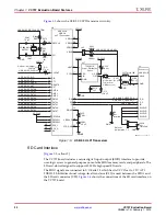
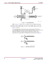
shows the shield for the USB mini-B connector (J2) can be tied to GND by a
jumper on header J44 pins 1–2 (default). The USB shield can optionally be connected
through a capacitor to GND by installing a tantalum capacitor (body size C) at location
C326 and jumping pins 2-3 on header J44.
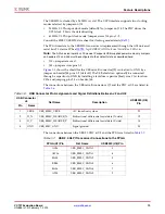
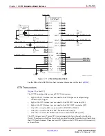
The connections between the USB mini-B connector at J2 and the PHY at U8 are listed in
The connections between the USB 2.0 PHY at U8 and the FPGA are listed in
Table 1-6:
USB Connector Pin Assignments and Signal Definitions Between J2 and U8
USB Connector
J2
Net Name
Description
USB3320 (U8)
Pin
Pin
Name
1
VBUS
USB_SMSC_VBUS
+5V from host system
22
2
D_N
USB_SMSC_HEADER_N
Bidirectional differential serial data (N-side)
19
3
D_P
USB_SMSC_HEADER_P
Bidirectional differential serial data (P-side)
18
4
GND
USB_SMC_GND
Signal ground
33
Table 1-7:
USB 2.0 ULPI Transceiver Connections to the FPGA
FPGA (U1) Pin
Net Name
USB3320 (U8) Pin
AV36
USB_SMSC_DATA0
3
AW36
USB_SMSC_DATA1
4
BA34
USB_SMSC_DATA2
5
BB34
USB_SMSC_DATA3
6
BA36
USB_SMSC_DATA4
7
AT34
USB_SMSC_DATA5
9

