

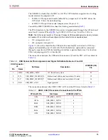


VC707 Evaluation Board
31
UG885 (v1.2) February 1, 2013
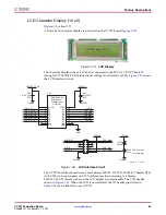
Feature Descriptions
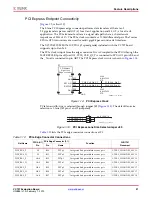
PCI Express Endpoint Connectivity
[
, callout
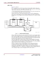
The 8-lane PCI Express edge connector performs data transfers at the rate of
2.5 gigatransfers per second (GT/s) for a Gen1 application and 5.0 GT/s for a Gen2
application. The PCIe transmit and receive signal datapaths have a characteristic
impedance of 85
Ω
±10%. The PCIe clock is routed as a 100
Ω
differential pair. The 7 series
FPGAs GTX transceivers are used for multi-gigabit per second serial interfaces.
The XC7VX485T-2FFG1761C FPGA (-2 speed grade) included with the VC707 board
supports up to Gen2 x8.
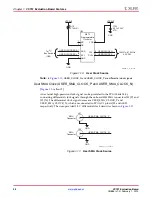
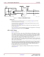
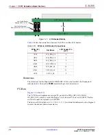
The PCIe clock is input from the edge connector. It is AC coupled to the FPGA through the
MGTREFCLK1 pins of Quad 115. PCIE_CLK_Q0_P is connected to FPGA U1 pin AB8, and
the _N net is connected to pin AB7. The PCI Express clock circuit is shown in
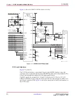
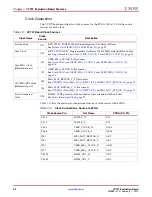
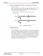
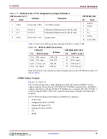
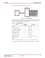
PCIe lane width/size is selected through jumper J49 (
). The default lane size
selection is 1-lane (J49 pins 1 and 2 jumpered).
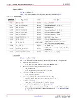
lists the PCIe edge connector connections at P1.
X-Ref Target - Figure 1-14
Figure 1-14:
PCI Express Clock
X-Ref Target - Figure 1-15
Figure 1-15:
PCI Express Lane Size Select Jumper J49
UG885_c1_14_020612
PCI Express
Eight-Lane
Edge connector
GND
GND
A15
A13
A14
P1
A12
GND
C544
0.01
μ
F 25V
X7R
C545
0.01
μ
F 25V
X7R
PCIE_CLK_Q0_P
PCIE_CLK_Q0_N
PCIE_CLK_Q0_C_P
PCIE_CLK_Q0_C_N
OE
REFCLK-
UG885_c1_15_020612
PCIE_PRSNT_B
PCIE_PRSNT_X1
PCIE_PRSNT_X4
PCIE_PRSNT_X8
J49
1
3
5
2
4
6
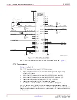
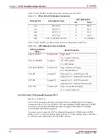
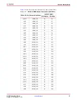
Table 1-12:
PCIe Edge Connector Connections
Net Name
FPGA (U1)
Pin
PCIe Edge Connector (P1)
Function
FHG1761
Placement
Pin
Name
PCIE_RX0_P
Y4
B14
PETp0
Integrated Endpoint block receive pair
GTXE2_CHANNEL_X0Y19
PCIE_RX0_N
Y3
B15
PETn0
Integrated Endpoint block receive pair
GTXE2_CHANNEL_X0Y19
PCIE_RX1_P
AA6
B19
PETp1
Integrated Endpoint block receive pair
GTXE2_CHANNEL_X0Y18
PCIE_RX1_N
AA5
B20
PETn1
Integrated Endpoint block receive pair
GTXE2_CHANNEL_X0Y18
PCIE_RX2_P
AB4
B23
PETp2
Integrated Endpoint block receive pair
GTXE2_CHANNEL_X0Y17
PCIE_RX2_N
AB3
B24
PETn2
Integrated Endpoint block receive pair
GTXE2_CHANNEL_X0Y17
PCIE_RX3_P
AC6
B27
PETp3
Integrated Endpoint block receive pair
GTXE2_CHANNEL_X0Y16