32
nd
Write
clock
pulse
1
st
Read
clock pulse
2
nd
Read
clock pulse
32
nd
Read
clock pulse
33
rd
Read
clock pulse
³(QG RI :ULWH &\FOH´
pulse
ReadBack
Data Bit31
Read
Back
Data
Bit29
Read
Back
Data
Bit1
ReadBack
Data Bit30
ReadBack
Data Bit0
³(QG RI :ULWH &\FOH´
pulse
DB 31 (MSB)
1
st
Write
clock
pulse
t
su1
t
h
t
( CLK)
32
nd
Write
clock
pulse
DB30
DB29
DB2
Address Bit2
DB1
Address Bit1
t
su2
t
w
DB0 (LSB)
Address Bit0
CLOCK
DATA
CLOCK
READBACK DATA
R
E
G
IS
T
E
R
W
R
IT
E
R
E
A
D
B
A
C
K
t
d
t
su2
t
w
LATCH
ENABLE
T
(CL)
T
(CH)
LATCH ENABLE
DB3
Address Bit3
34
SLWS245B – MAY 2014 – REVISED FEBRUARY 2017
Product Folder Links:
Copyright © 2014–2017, Texas Instruments Incorporated
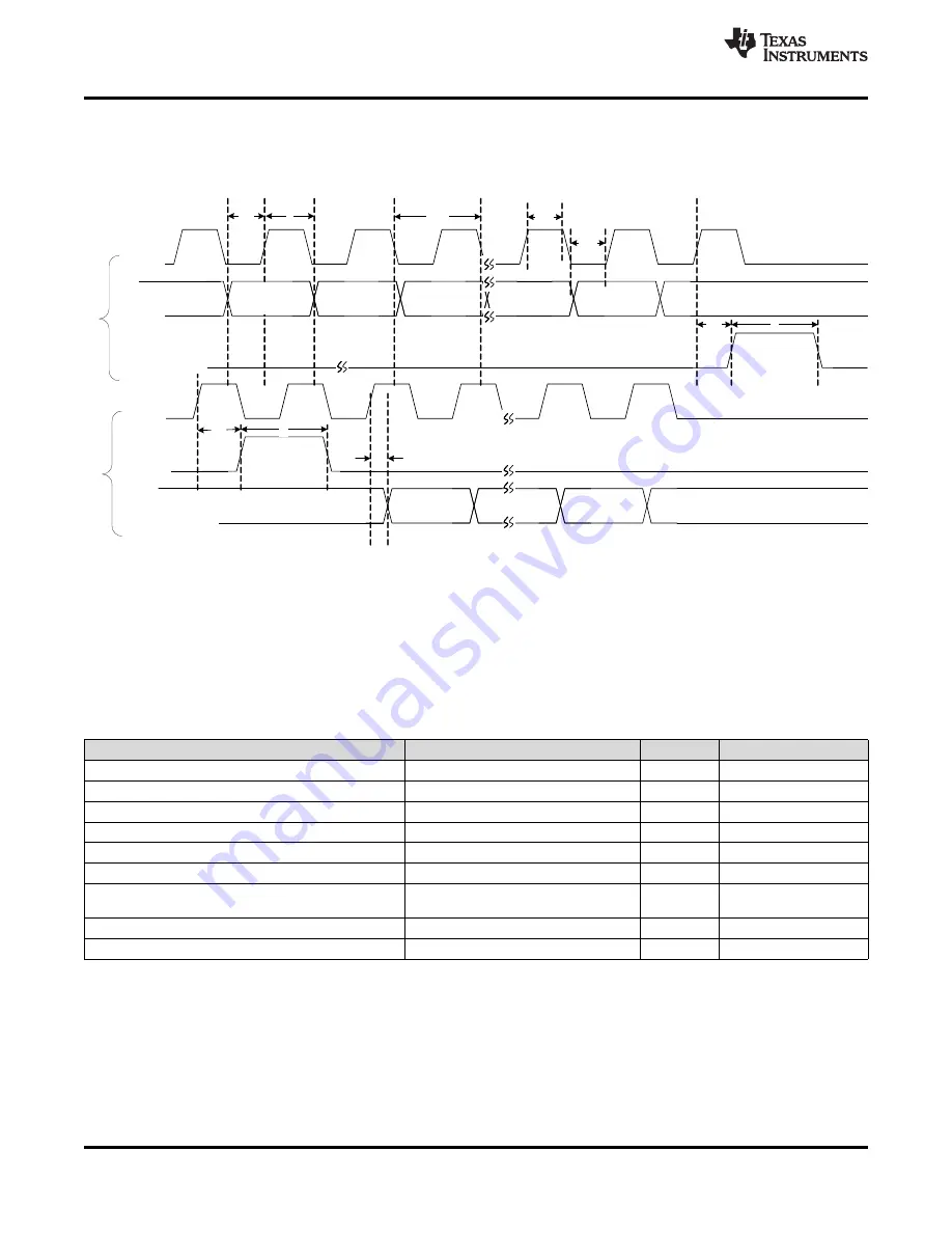
TRF3722 integrates 7 registers: Register 0 (000) to Register 6 (110). Registers 1 through 6 are used to set-up
and control the TRF3722 functionalities, while register 0 is used for the read-back function. Each read-back is
composed by two phases: writing followed by the actual reading of the internal data. This is shown in the timing
diagram in
Figure 131. 4WI Read-Back Timing Diagram
During the writing phase a command is sent to TRF3722 register 0 to set it in read-back mode and to specify
which register is to be read. In the proper reading phase, at each rising clock edge, the internal data is
transferred into the RDBK pin and can be read at the following falling edge (LSB first). The first clock after the LE
goes high (end of writing cycle) is idle and the following 32 clocks pulses will transfer the internal register content
to the RDBK pin.
shows the Readback timing.
Table 2. 4WI Timing for Readback Timing
MIN
TYP
MAX
UNIT
COMMENT
t
h
Hold time, data to clock
20
ns
t
SU1
Setup time, data to clock
20
ns
t
CH
Clock low duration
20
ns
t
CL
Clock High duration
20
ns
t
SU2
Setup time, clock to enable
20
ns
t
SU3
Setup time, enable to Readback clock
20
ns
t
d
Delay time, clock to Readback data
output
10
t
W
Enable Time
50
ns
Equals Clock period
t
(CLK)
Clock period
50
ns


