Register Descriptions
A-4
A.2 Register Descriptions
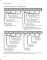
The following figures summarize the content of the ’C2xx status and control
registers that are divided into fields. (The other registers contain no control
bits; they simply hold a single 16-bit value.) Each figure in this section provides
information in this way:
-
The value shown in the register is the value after reset. If the value of a
particular bit is not affected by reset or depends on pin levels at reset, that
bit will contain an X.
-
Each unreserved bit field or set of bits has a callout that very briefly de-
scribes its effect on the processor.
-
Each non-reserved bit field or set of bits is labeled with one or more of the
following symbols:
J
R indicates that your software can read the bit field but cannot write to
it.
J
W indicates that your software can read the bit field and write to it.
J
W1C indicates that writing a 1 to the bit field clears it to 0; writing a 0
has no effect.
When both read access and write access apply to a bit field, two of these
symbols are shown, separated by / (a forward slash): R/W or R/W1C.
-
Where needed, footnotes provide additional information for a particular
figure.


