Index
Index-7
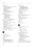
data memory select pin (DS)
definition
4-3
shown in figure
4-10, 4-13
data page 0
4-8
caution about test/emulation addresses
4-8
data page pointer (DP)
caution about initializing DP
6-5
definition
3-16
load (LDP instruction)
7-83
role in direct addressing
6-4
data read bus (DRDB)
2-3
data write bus (DWEB)
2-3
data-read address bus (DRAB)
2-3
data-scaling shifter
at input of CALU
3-3
at output of CALU
3-11
data-write address bus (DWAB)
2-3
delta interrupts
description
10-17
enabling/disabling (DIM bit)
10-8
device reset
5-33
diagnostic applications
E-24
digital loopback mode
9-28
DIM bit
10-8
dimensions
12-pin header
E-20
14-pin header
E-14
mechanical, 14-pin header
E-14
DIO0–DIO3 (bits), detecting change on pins
IO0–IO3
10-16
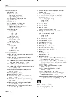
direct addressing
description
6-4
examples
6-6
figure
6-5
opcode format
6-5 to 6-7
role of data page pointer (DP)
6-4
direct memory access (using HOLD opera-
tion)
4-27
during reset
4-29
example
4-28
terminating correctly
4-29
DIV1 and DIV2 pins
8-5, F-7
divide (SUBC instruction)
7-180
DLB bit
9-12
DMOV instruction
7-66
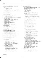
DP (data page pointer)
caution about initializing DP
6-5
definition
3-16
load (LDP instruction)
7-83
role in direct addressing
6-4
DR bit
10-11
DR pin
9-4
DRAB (data-read address bus)
2-3
DRDB (data read bus)
2-3
DS (data memory select pin)
definition
4-3
shown in figure
4-10, 4-13
DSWS bit(s)
’C203/C204
8-15
’C209
11-17
dual-access RAM (DARAM)
F-6
configuration
’C203
4-33
’C204
4-36
’C209
11-8
description
2-7
DuPont connector
E-2
DWAB (data-write address bus)
2-3
DWEB (data write bus)
2-3
DX pin
9-4
E
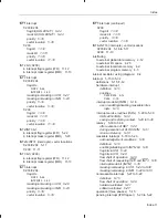
EMU0/1
configuration
E-21, E-23, E-24
emulation pins
E-20
IN signals
E-21
rising edge modification
E-22
EMU0/1 signals
E-2, E-3, E-6, E-7, E-13, E-18
emulation
configuring multiple processors
E-13
JTAG cable
E-1
pins
E-20
timing calculations
E-7 to E-9, E-18 to E-26
using scan path linkers
E-16
emulation capability
2-13
emulation modes (FREE and SOFT bits)
asynchronous serial port
10-7
synchronous serial port
9-8
timer
8-11
emulation timing
E-7

