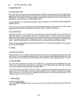
Circuit Description
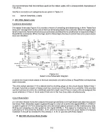
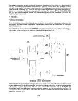
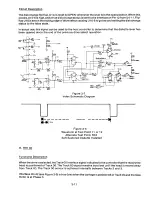
Data is sent to the drive via interface Pin 38. This signal is inverted by U22, and is used to clock the D
flip flop U23. The outputs of U23 are inverted subsequently, and used to drive Q15 and Q17, which
direct the write current to the correct winding.
F. TRIM ERASE
Functional Description
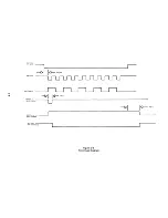
The TM848 uses a tunnel erase scheme to achieve trim erase, which is used to erase a guard band
around the data tracks, allowing minor track offsets and minor misalignment without data errors
occurring. The erase poles are staggered.036 inch behind the read/write poles. At a media rotational
speed of 360 RPM, the tunnel erase method requires that the trim erase be delayed for 190
microseconds afer the start of writing and that it be continued for 550 microseconds after the end of
writing the data. The two one shots in U30 provide these delay time intervals.
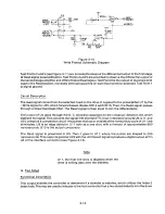
When the write gate goes low, U30, Pin 9, (A input), is triggered and a high to low to high transition of
190 us is generated. The write gate is also applied to U30 P in 1 (A input). When the write data is
applied to the WRT DATA line, U23 c o n d itions the data w h ich in t urn ge ne rates the signal WRT
TRAN+ (write tra). This signal is then applied to U30 Pin 2, (B input) which is a positive
triggered input. This clock will retrigger this one shot continuously until the last transition of the WRT
TRAN+ and WRT GATE — occurs. At this time, the one shot stays on for an additional 550 us. These
outputs (U30, Pins 12 and 13) are gated by U31 which is the trime erase gate. This output goes low
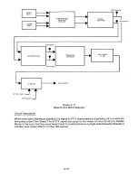
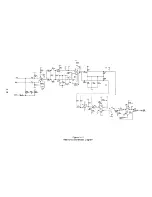
whenever both inputs are high, causing the trim erase to be enabled (see Figure 3-5).
G. SIDE SELECT
Functional Description
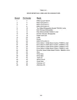
SIDE SELECT can be generated three ways. See the option listing, Section 1.19, for this information.
*
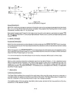
When the Side Select signal is low, Side 1 (the upper head) of the drive is selected for read/write
operations. When this signal is high, Side 0 of the drive is selected (see Figure 3-6). The Side Select
signal must be stable during an entire read or write operation. This signal is best implemented in
synchronization with the Drive Select line signal.
Circuit Description
As shipped from the factory, the Side Select signal is received on Pin 14 of edge connector P13. This
signal is received by U22, inverted, then inverted again by U13. The output of U13, Pin 10, generates
the signal called Side 1 —.
The Side 1 — signal is applied to U13, Pin 9, and U24, Pin 13. The output of U13, Pin 8, is applied to U24,
Pin 1. This output at Pin 2 of U24 is the opposite of U24, Pin 12. The resistor divider network sets up
the biasing voltages to turn on and turn off the head select transistor, Q18 or Q19. The head biasing
voltages seen across the collector resistors will be 5.2V D. C. when selecting a head for a read
operation, 12V D.C. during a write operation, and OV D. C. when the head is not selected. The emitter
voltages on Q18 and Q19 will always be the opposite of each other, causing CTO or CT1 (center tap 0,
center tap 1) to be selected.
3-7
Summary of Contents for TM848-1
Page 32: ...HUB CENTER LINE TRACK 0 TRACK 38 TRACK 76 Figure 2 2 Hub Center Line and Track Locations 2 3 ...
Page 81: ...APPENDIX I PRINTED CIRCUIT BOARD S CHEM A T ICS AND ASSEM B LY DRAW IN G S ...
Page 88: ...APPENDIX II RECOM M E N D E D SPARE PARTS LIST ...
Page 90: ...Pi N 1 79031 001 1 082 ...

