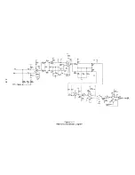
Circuit Description
The Direction line comes in on Pin 34 of the interface connector. A high signal directs the step logic to
step toward Track 00. A low signal directs the step logic to step toward a higher numbered track.
The direction line sets the proper phase to the exclusive OR gates of U9.
TABLE 3-2
STEPPER LOGIC TRUTH TABLE
Step Out Toward Track 00
Step In Toward The
Pin No.
U21-9
U21-8
U21-5
U21-6
Phase
0
3
2
1
0
Pin No.
0
1
0
1
1
0
0
0
0
1
0
0
1
1
1
1
0
0
1
1
0
0
1
1
1
0
0
1
1
0
Upper Tracks
Phase
2
3
0
1
1
0
0
0
1
1
0
0
0
1
1
U21-9
U21-8
U21-5
U21-6
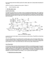
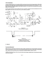
The step pulses come in at Pin 36 of the interface connector. They are buffered by U22 and gated at
U14 by the unit select, and the Not Write signal. The step pulses then go to the C inputs of the two flip
flops at U21. The direction of the step, hence the selection of the flip flop to be toggled, is done by the
two exclusive OR gates of U9. These gates are controlled by the step direction line and by the state of
the two flip flop outputs.
The POR- (Power On Reset) signal resets the two flip' flops to Phase 0 after a Power On.
The output of the two flip flops drives the stepper motor through the drivers of U39, U40, and U12. The
diodes, CR2-9, are for voltage spike e l imination. The current t h rough th e s t e p per mo tor c o ils is
reversed sequentially, one at a time.
D. WAX"GITE
Functional Description
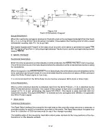
When the Write Gate signal is true (low), the write electronics are prepared for writing data (read
electronics disabled). This signal turns on the write current in the read/write head. Data is written
under control of the Write Data input line. It is necessary for the Write Gate interface line to go low
before the first Write Data pulse. However, the separation between the leading edge of Write Gate
and the first significant Write Data pulse should not be less than two microseconds and not greater
than four microseconds. The same restrictions exist for the relationship between the last Write Data
pulse and the termination of the W r ite G ate signal. When the Write Gate line goes false (high), the
trim erase will stay on for 550 microseconds (see Trim Erase, page 3-7).
When a w r i t e -protected d i s k ett e i s i n s t a l led i n t h e d r i ve, th e w r i t e e l e c t r o nics ar e d i s a b led,
irrespective of th e s t at e o f t h e W r ite Gate l i ne. Check th e l ist of o p t i ons (see Section 1.19) for
exceptions and further discussion of write protect options. Stepping is also disabled by a true (low)
Write Gate.
Tendon Corporation recommends that the controller wait one millisecond after the WWRWATE goes
high (false) before any step pulses are sent to the drive.
C ircuit Descri t i o n
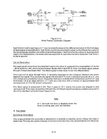
A low (true) WRT GATE signal is applied to Pin 40 o f th e i n t erface co nnector P13. This signal is
3-5
Summary of Contents for TM848-1
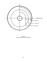
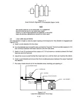
Page 32: ...HUB CENTER LINE TRACK 0 TRACK 38 TRACK 76 Figure 2 2 Hub Center Line and Track Locations 2 3 ...
Page 81: ...APPENDIX I PRINTED CIRCUIT BOARD S CHEM A T ICS AND ASSEM B LY DRAW IN G S ...
Page 88: ...APPENDIX II RECOM M E N D E D SPARE PARTS LIST ...
Page 90: ...Pi N 1 79031 001 1 082 ...

