The Trim Erase control goes true 190 microseconds after the Write Enable interface line
since the trim erase gaps are behind the read/write gap. It should be noted that this value is
optimized between the requirements at Track 00 and at Track 76, so that the effect of the trim
erase gaps on previous information is minimized.
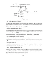
Figure 1-4 shows the information on the write data interface line and the output of the write
waveform generator, which toggles on the leading edge of every write data pulse.
A maximum of 4 microseconds between write gate going true and the first write data pulse is
only required if faithful reproduction of the first write data transition is signifcant.
At the end of recording, at least one additional pulse on the write data line must be inserted
after the last significant write data pulse to avoid excessive peak shift effects.
NOTE 1
I
NOTE 2
WRITE GATE
190 u sec
I
~ 5
0 u s e c ~
I
TRIM E:RASE
INTERNAL WRITE
BUSY
I
WRITE DATA
I
I
NOTE 2
I
WRITE
WAVEFORM
GENERATOR
I
I
I
WRITE CURRENT
- N OTE 3
NOTE 4
Q
1=0
NOTES:
1,
T
= 0 700 MILLISECOND S AFTER DRIVE MOTO R
STARTS OR 20 MILLISECONDS AFTER LAST STEP
PULSE, WHICHEVER IS THE LATEST TIME.
3.
1 0 M A PEAK TO PEAK, TRACK 0 TO
TRACK 42; 7.5 MA PEAK TO PEAK
TRACK 43 TO TRACK 77.
2.
UNS Y C H RONIZED
4. 2 U S EC MINIMUM
4 USEC MAXIMUM
Figure 1-4
Write Operation Timing Diagram
The duration of a write operation is from the true going edge of write gate to the false going edge of
erase. This is indicated by the internal write busy waveform shown (see Figure 1-4).
The Read electronics consist of:
1, Read Switch/Side Select
2. Read Preamplifier
3. Filter
4. Differentiatior
5. Time Domain Filter and Digitizer
The read switch is used to isolate the read amplifier from the voltage excursion across the head
during a write operation. The side select is used to enable one of the read/write/erase heads.
The drive must be in a ready condition before reading can begin. As with the data recording operation,
this ready c o n d ition m us t b e e s t a b l ished b y t h e u s e r s y s t em. ln a d d i t ion t o t h e r e q u i rements
established in this section, a period of 100 microseconds is necessary after a trim erase operation
occurs to allow the read amplifier to settle after the transient caused by the read switch returning to
the read mode.
1-11
Summary of Contents for TM848-1
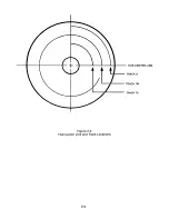
Page 32: ...HUB CENTER LINE TRACK 0 TRACK 38 TRACK 76 Figure 2 2 Hub Center Line and Track Locations 2 3 ...
Page 81: ...APPENDIX I PRINTED CIRCUIT BOARD S CHEM A T ICS AND ASSEM B LY DRAW IN G S ...
Page 88: ...APPENDIX II RECOM M E N D E D SPARE PARTS LIST ...
Page 90: ...Pi N 1 79031 001 1 082 ...

