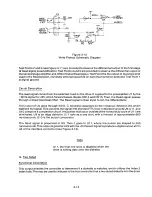
inverted and gated with Write Protect and Drive Select to enable U23, U30, and Q13. Transistors Q13
and Q12 are write current switches. Q13 and Q12 are on in parallel when the low Write Current
interface is high (false). This results in a write current of 10 milliamps. When the low Write Current line
goes low (true), transistor Q12 turns off, and the current decreases to 7 milliamps. R52 and R51
determine the amount of write current supplied to the head. The network CR18, CR19, CR20, R80
and R81 is a power-loss write disable. If a sudden voltage loss occurs, transistor Q14 turns off,
disabling the write current.
E. WRT DATA
Functional Description
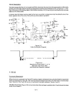
When the drive is selected, the write data line provides the bit-serial Write Data pulses that control the
switching of the write current in the heads. The write electronics must be conditioned for writing by
the Write Gate line.
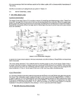
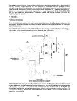
For each high-to-low transition on the WRT DATA line, a flux change is produced at the head write gap.
This causes a flux change to be stored on the diskette (see Figure 3-4).
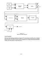
N INTERNAL WRITE BUSY
SELECT
LOGIC
SIDE
SELECT
READ/
WRITE
COILS
WRITE
DRIVER I
WRITE
DATA
TRIGGER
WRITE
DRIVER 2
ERASE
COIL
NWRITE GATE
N WRITE PROTECT
UNIT SELECT
IN WRITE)
WRITE
CURRENT
SOURCE
ERASE
DELAY
LOGIC
ERASE
CURRENT
SOURCE
IN INTERNAL ~
R E A D DISABLE
WRITE BUSY)
Figure 3-4
Write Data Circuit Block Diagram
When a double-frequency type encoding technique is used (in which data and clock form the combined
Write Data signal), it is recommended that the repetition of the high-to-low transitions, when writing
all zeros, be equal to the nominal data rate +0.1 percent. The repetition rate of the high-to-low
transitions, when writing all ones, should be equal to twice the nominal data rate +0.1 percent. The
data transfer rate for a 1F pattern is 250,000 Bits Per Second (BPS). The data transfer rate for a 2F
pattern is 500,000 BPS.
3-6
Summary of Contents for TM848-1
Page 32: ...HUB CENTER LINE TRACK 0 TRACK 38 TRACK 76 Figure 2 2 Hub Center Line and Track Locations 2 3 ...
Page 81: ...APPENDIX I PRINTED CIRCUIT BOARD S CHEM A T ICS AND ASSEM B LY DRAW IN G S ...
Page 88: ...APPENDIX II RECOM M E N D E D SPARE PARTS LIST ...
Page 90: ...Pi N 1 79031 001 1 082 ...

