


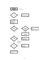


6-10E
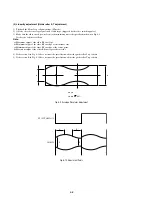
(4) Envelope Check
1) Make recordings on T-120 (E-120) and T-160 (E-180) tape.
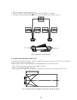
Make sure the playback output envelope meets the specification as shown in Fig. 6-13.
2) Play back a self recorded tape (recording made on the unit using with T-120 (E-120).
The video envelope should meet the specification as shown in Fig. 6-13.
In SP mode, (A) should equal (B).
If the head gap is wide, upper cylinder should be checked.
Fig. 6-13 Envelope Input and Output Level
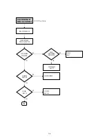
(5) Tape Wrinkle Check
1) Run the T-160 (E-180) tape in the playback, FPS, RPS and Pause modes and observe tape wrinkle at each guide.
2) If excessive tape wrinkle is observed, perform the following adjustments in Playback mode :
◆
Tape wrinkle at the guide roller S, T section : Linearity adjustment.
◆
Tape wrinkle at tape guide flange : ACE head assembly coarse adjustment.
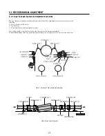
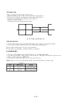
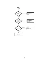
6-2-3 Reel Torque
1) The rotation of the capstan motor causes the holder clutch ass’y to rotate through the belt pulley.
2) The spring wrap PLAY/REV of holder clutch ass’y drives the disk reel S, T through gear idler by rotation of gear center ass’y.
3) Brake is operated by slider cam at FF/REW mode.
4) Transportation of accurate driving force is done by gears. (Gear Center Ass’y)
Note:
If the spec. does not meet the followings specifications, replace the holder clutch ass’y and then recheck.
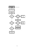
< Table 6-1 >
MODE
TORQUE g/cm
GAUGE
PB
42
±
11
Cassette Torquemeter
RPS
145
±
30
Cassette Torquemeter
A
B
Summary of Contents for RDR VX555 - DVDr/ VCR Combo
Page 62: ...2 22 2 22E MEMO ...
Page 64: ...3 4E MEMO ...
Page 66: ...4 1 DVD Main PCB 4 4 4 3 COMPONENT SIDE ...
Page 67: ...4 6 4 5 CONDUCTOR SIDE ...
Page 68: ...4 8 4 7 4 2 VCR Main PCB COMPONENT SIDE ...
Page 69: ...4 10 4 9 CONDUCTOR SIDE ...
Page 70: ...4 12 4 11 4 3 Function PCB COMPONENT SIDE COMPONENT SIDE ...
Page 71: ...4 14 4 13 4 4 Front Jack PCB COMPONENT SIDE CONDUCTOR SIDE ...
Page 72: ...4 16E 4 15 4 5 DV Jack PCB COMPONENT SIDE COMPONENT SIDE ...
Page 74: ...5 4 5 3 5 1 S M P S VCR Main PCB ...
Page 75: ...5 6 5 5 5 2 Power VCR Main PCB ...
Page 76: ...5 8 5 7 5 3 Logic VCR Main PCB ...
Page 77: ...5 10 5 9 5 4 A V VCR Main PCB ...
Page 78: ...5 12 5 11 5 5 Hi Fi VCR Main PCB ...
Page 79: ...5 14 5 13 5 6 MPEG Decoder DVD Main PCB ...
Page 80: ...5 16 5 15 5 7 A V Decoder DVD Main PCB ...
Page 81: ...5 18 5 17 5 8 In Out DVD Main PCB ...
Page 82: ...5 20 5 19 5 9 DV HDMI DVD Main PCB ...
Page 83: ...5 22 5 21 5 10 Front Timer Front Jack PCB DV Jack DV Jack PCB ...
Page 84: ...5 24E 5 23 5 11 Function Function PCB ...
Page 127: ...MEMO ...


