


6-4
6-2 VCR MECHANICAL ADJUSTMENT
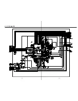
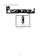
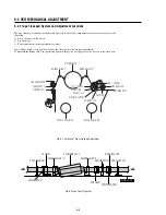
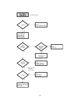
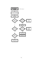
6-2-1 Tape Transport System and Adjustment Locations
The tape transport system has been adjusted precisely in the factory. Alignment is not necessary except for the
following :
1) Noise observed on the screen.
2) Tape damage.
3) Parts replacement in the tape transport system.
Lower flange height of tape guide is used as the reference for the transport adjustment.
To maintain the height of the tape guide and prevent damage, do not apply excessive force onto the main base.
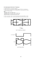
Fig. 6-4 Tape Travel Diagram
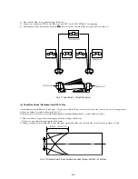
POST TENSION
MAIN BASE
FE HEAD
CYLINDER ASS'Y
PINCH ROLLER
GUIDE ROLLER "S"
GUIDE ROLLER "T"
#8 GUIDE POST #9 GUIDE POST
CAPSTAN SHAFT
ACE HEAD
#3 GUIDE POST
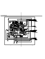
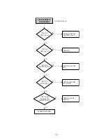
Fig. 6-3 Location of Tape Transport Adjustment
TENSION POST
#3 GUIDE POST
GUIDE ROLLER "S"
SUPPLY REEL DISK
FULL ERASE HEAD
TI LT SCREW
AZIMUTH SCREW
X-POSITION
ADJUS T SLIT
TAKE UP REEL DISK
CYLINDER ASS' Y
GUIDE ROLLER "T"
#8 GUIDE POST
#9 GUIDE POST
PINCH ROLLER
HIGH T SCREW
CAPSTAN
Summary of Contents for RDR VX555 - DVDr/ VCR Combo
Page 62: ...2 22 2 22E MEMO ...
Page 64: ...3 4E MEMO ...
Page 66: ...4 1 DVD Main PCB 4 4 4 3 COMPONENT SIDE ...
Page 67: ...4 6 4 5 CONDUCTOR SIDE ...
Page 68: ...4 8 4 7 4 2 VCR Main PCB COMPONENT SIDE ...
Page 69: ...4 10 4 9 CONDUCTOR SIDE ...
Page 70: ...4 12 4 11 4 3 Function PCB COMPONENT SIDE COMPONENT SIDE ...
Page 71: ...4 14 4 13 4 4 Front Jack PCB COMPONENT SIDE CONDUCTOR SIDE ...
Page 72: ...4 16E 4 15 4 5 DV Jack PCB COMPONENT SIDE COMPONENT SIDE ...
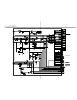
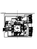
Page 74: ...5 4 5 3 5 1 S M P S VCR Main PCB ...
Page 75: ...5 6 5 5 5 2 Power VCR Main PCB ...
Page 76: ...5 8 5 7 5 3 Logic VCR Main PCB ...
Page 77: ...5 10 5 9 5 4 A V VCR Main PCB ...
Page 78: ...5 12 5 11 5 5 Hi Fi VCR Main PCB ...
Page 79: ...5 14 5 13 5 6 MPEG Decoder DVD Main PCB ...
Page 80: ...5 16 5 15 5 7 A V Decoder DVD Main PCB ...
Page 81: ...5 18 5 17 5 8 In Out DVD Main PCB ...
Page 82: ...5 20 5 19 5 9 DV HDMI DVD Main PCB ...
Page 83: ...5 22 5 21 5 10 Front Timer Front Jack PCB DV Jack DV Jack PCB ...
Page 84: ...5 24E 5 23 5 11 Function Function PCB ...
Page 127: ...MEMO ...


