


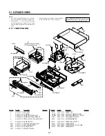


7-29
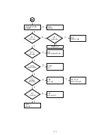
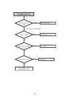
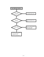
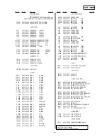
Line1 CVBS Video Input Error
Check JK801
(Video input signal)
No
Check VCC of AVIC1 and peripheral
parts of Clock oscillation
(Pin #53, 54) of AVIC1
No
Yes
Yes
Check AVIC1
(Pin # 15)
Check VCC and peripheral parts of
AVIC1
No
Yes
Check AVIC1
(Pin #75, 76, 79 ~ 84)
Check peripheral parts of JK801
1. Check VCC of IC101 and peripheral
parts of Clock oscillation
(IC105 Pin #1, 2, 14)
2. Refer to the “ CVBS output error”
Summary of Contents for RDR VX555 - DVDr/ VCR Combo
Page 62: ...2 22 2 22E MEMO ...
Page 64: ...3 4E MEMO ...
Page 66: ...4 1 DVD Main PCB 4 4 4 3 COMPONENT SIDE ...
Page 67: ...4 6 4 5 CONDUCTOR SIDE ...
Page 68: ...4 8 4 7 4 2 VCR Main PCB COMPONENT SIDE ...
Page 69: ...4 10 4 9 CONDUCTOR SIDE ...
Page 70: ...4 12 4 11 4 3 Function PCB COMPONENT SIDE COMPONENT SIDE ...
Page 71: ...4 14 4 13 4 4 Front Jack PCB COMPONENT SIDE CONDUCTOR SIDE ...
Page 72: ...4 16E 4 15 4 5 DV Jack PCB COMPONENT SIDE COMPONENT SIDE ...
Page 74: ...5 4 5 3 5 1 S M P S VCR Main PCB ...
Page 75: ...5 6 5 5 5 2 Power VCR Main PCB ...
Page 76: ...5 8 5 7 5 3 Logic VCR Main PCB ...
Page 77: ...5 10 5 9 5 4 A V VCR Main PCB ...
Page 78: ...5 12 5 11 5 5 Hi Fi VCR Main PCB ...
Page 79: ...5 14 5 13 5 6 MPEG Decoder DVD Main PCB ...
Page 80: ...5 16 5 15 5 7 A V Decoder DVD Main PCB ...
Page 81: ...5 18 5 17 5 8 In Out DVD Main PCB ...
Page 82: ...5 20 5 19 5 9 DV HDMI DVD Main PCB ...
Page 83: ...5 22 5 21 5 10 Front Timer Front Jack PCB DV Jack DV Jack PCB ...
Page 84: ...5 24E 5 23 5 11 Function Function PCB ...
Page 127: ...MEMO ...


