


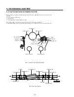


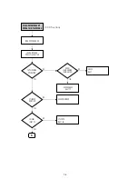


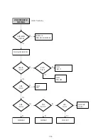

6-9
6) Play back the Mono Scope alignment tape (SP mode).
7) Connect an oscilloscope CH-1 to the “Envelope” and CH-2 to the “H’D SW Pulse” for triggering.
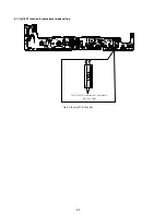
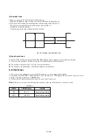
8) Turn the guide roller heads with a flat head (
) driver to obtain a flat video RF envelope as shown in Fig. 6-11.
Fig. 6-11 Guide Roller S, T Height Adjustment
IDEAL ENVELOPE
S HEIGHT TOO HIGH
S HEIGHT TOO LOW
T HEIGHT TOO HIGH
T HEIGHT TOO LOW
GUIDE ROLLER S
GUIDE ROLLER T
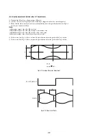
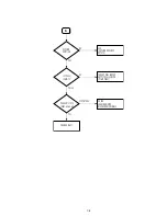
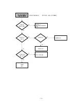
Fig. 6-12 Video Envelope Rising when Operation mode Changes from RPS to Play Mode
ENTRANCE SIDE ENVELOPE
(3) Check Transitional Operation from RPS to Play
Check transition from RPS mode to play mode : Using a pre-recorded SP tape, make sure the entry side of envelope comes to an appropriate
steady state within 3 seconds (as shown in Fig. 6-12).
If the envelope waveform does not reach specified peak-to peak amplitude within 3 seconds, adjust as follows :
1) Make sure there is no gap between the supply roller lower flange and the tape.
If there is a gap, adjust the supply guide roller again.
2) Change operation mode from the RPS to the play mode (again) and make sure the entry side of envelope rises within 3 second.
Summary of Contents for RDR VX555 - DVDr/ VCR Combo
Page 62: ...2 22 2 22E MEMO ...
Page 64: ...3 4E MEMO ...
Page 66: ...4 1 DVD Main PCB 4 4 4 3 COMPONENT SIDE ...
Page 67: ...4 6 4 5 CONDUCTOR SIDE ...
Page 68: ...4 8 4 7 4 2 VCR Main PCB COMPONENT SIDE ...
Page 69: ...4 10 4 9 CONDUCTOR SIDE ...
Page 70: ...4 12 4 11 4 3 Function PCB COMPONENT SIDE COMPONENT SIDE ...
Page 71: ...4 14 4 13 4 4 Front Jack PCB COMPONENT SIDE CONDUCTOR SIDE ...
Page 72: ...4 16E 4 15 4 5 DV Jack PCB COMPONENT SIDE COMPONENT SIDE ...
Page 74: ...5 4 5 3 5 1 S M P S VCR Main PCB ...
Page 75: ...5 6 5 5 5 2 Power VCR Main PCB ...
Page 76: ...5 8 5 7 5 3 Logic VCR Main PCB ...
Page 77: ...5 10 5 9 5 4 A V VCR Main PCB ...
Page 78: ...5 12 5 11 5 5 Hi Fi VCR Main PCB ...
Page 79: ...5 14 5 13 5 6 MPEG Decoder DVD Main PCB ...
Page 80: ...5 16 5 15 5 7 A V Decoder DVD Main PCB ...
Page 81: ...5 18 5 17 5 8 In Out DVD Main PCB ...
Page 82: ...5 20 5 19 5 9 DV HDMI DVD Main PCB ...
Page 83: ...5 22 5 21 5 10 Front Timer Front Jack PCB DV Jack DV Jack PCB ...
Page 84: ...5 24E 5 23 5 11 Function Function PCB ...
Page 127: ...MEMO ...


