5-33
1-6.
SYSTEM CONTROL SYSTEM ADJUSTMENTS
1. Battery Down Adjustment
Set the battery end voltage.
If the voltage is incorrect, the life of battery will shorten.
The image at the battery end will also be rough.
Mode
STILL
Subject
Arbitrary
Measurement Point
Displayed data of page: 2,
address: 51
Measuring Instrument
Adjusting remote commander
Adjustment Page
D
Adjustment Address
90 to 94
Connection:
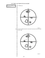
1) Connect the regulated power supply and the digital voltmeter
to the battery terminal as shown in Fig. 5-1-27.
Preparations before adjustment:
1) Adjust the output voltage of the regulated power supply so
that the digital voltmeter display is 3.6 ± 0.1 Vdc.
2) Turn off the power supply.
3) Turn the HOLD switch of the adjusting remote commander.
4) Turn on the power supply.
5) Insert the memory stick to the unit, and set the STILL mode.
6) Set the FOCUS switch in MANUAL mode.
Adjusting method:
Order Page Address Data
Procedure
1
0
01
01
2
6
2C
01
Decrease the output voltage
3
of the regulated power supply
so that digital voltmeter display
is 3.1 ± 0.01 Vdc.
Check the data.
4
2
51
74 to 86 : Normal
00 to 73, 87 to FF: Defective
5
2
51
Read the data, and this data
is named Dref.
6
D
90
Dref
Press PAUSE button.
7
Convert Dref to decimal notati
on and obtain Dref’. (Note)
Calculate D
91
’, D
92
’, D
93
’
and D
94
’ using following
equations(decimal calculation)
8
D
91
’=Dref’+3
D
92
’=Dref’+10
D
93
’=Dref’+10
D
94
’=Dref’+10
Convert D
91
’, D
92
’, D
93
’ and
9
D
94
’ to a hexadecimal number,
and obtain D
91
, D
92
, D
93
and
D
94
(Note)
10
D
91
D
91
Press PAUSE button.
11
D
92
D
92
Press PAUSE button.
12
D
93
D
93
Press PAUSE button.
13
D
94
D
94
Press PAUSE button.
Note:
Refer to table 5-2-2. “Hexadecimal-decimal conversion
table”
Processing after Completing Adjustments:
Order Page Address Data
Procedure
1
6
2C
00
2
0
01
00
PD-137 board
CN881
1
18
Regulated power supply
(6.0 to 7.2 Vdc)
CPC-9jig
(J-6082-393-C)
Adjusting remote
commander
BT-2 board
Regulated power supply
(3.1
±
0.01 Vdc)
Digital voltmeter
CN001
qa
pin
CN001
qd
pin
1
18
Fig. 5-1-27


