Silicon Laboratories Si4430 Manual Download Page 56

S i 4 4 3 0

56

Preliminary Rev. 0.4

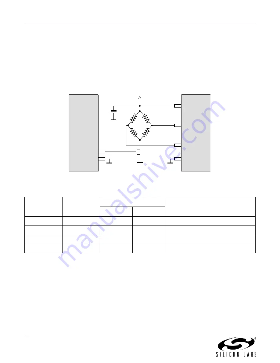
8.3.1. ADC Differential Input Mode—Bridge Sensor Example

The differential input mode of ADC8 is designed to directly interface any bridge-type sensor, which is demonstrated
in the figure below. As seen in the figure the use of the ADC in this configuration will utilize two GPIO pins. The
supply source of the bridge and chip should be the same to eliminate the measuring error caused by battery
discharging. For proper operation one of the VDD dependent references (VDD/2 or VDD/3) should be selected for
the reference voltage of ADC8. VDD/2 reference should be selected for VDD lower than 2.7 V, VDD/3 reference
should be selected for VDD higher than 2.7 V. The differential input mode supports programmable gain to match
the input range of ADC8 to the characteristic of the sensor and VDD proportional programmable offset adjustment
to compensate the offset of the sensor.

Figure 25. ADC Differential Input Example—Bridge Sensor

The adcgain[1:0] bits in "Register 0Eh. I/O Port Configuration" determine the gain of the differential/single ended
amplifier. This is used to fit the input range of the ADC8 to bridge sensors having different sensitivity:

Note:

The input range is the differential voltage measured between the selected GPIO pins corresponding to the full ADC
range (255). 
The gain is different for different VDD dependent references so the reference change has no influence on input range
and digital measured values.

adcgain[1]

adcgain[0]

Differential Gain

Input Range (% of VDD)

adcref[0] = 0

adcref[0] = 1

0

0

22/13

33/13

16.7

0

1

44/13

66/13

8.4

1

0

66/13

99/13

5.6

1

1

88/13

132/13

4.2

GPIO2

GPIO1

VDD

GND

Digital I/O

measure control

Tamara

Microcontroller

+        -

+

GND

Summary of Contents for Si4430

Page 1: ...he Si4430 s digital receive architecture features a high performance ADC and DSP based modem which performs demodulation filtering and packet handling for increased flexibility and performance This di...

Page 2: ...I Controller Digital Logic PFD PWR_CTRL TX RFn PA_RAMP PWR_CTRL PA_RAMP GPIO_2 GPIO_1 TXMOD Xout Xin Digital Modem Digital LDO RC 32K OSC 30M XTAL OSC RF LDO IF LDO VCO LDO PLL LDO BIAS SDN TXRXSW ANT...

Page 3: ...Mode 33 4 4 Direct Mode 33 4 5 PN9 Mode 34 4 6 Synchronous vs Asynchronous 34 5 Internal Functional Blocks 36 5 1 RX LNA 36 5 2 RX I Q Mixer 36 5 3 Programmable Gain Amplifier 36 5 4 ADC 36 5 5 Digita...

Page 4: ...60 8 6 Wake Up Timer 61 8 7 Low Duty Cycle Mode 63 8 8 GPIO Configuration 64 8 9 Antenna Diversity 65 8 10 RSSI and Clear Channel Assessment 66 9 Reference Design 67 10 Measurement Results 69 11 Appli...

Page 5: ...ter Encoding and CRC 45 Figure 23 POR Glitch Parameters 53 Figure 24 General Purpose ADC Architecture 55 Figure 25 ADC Differential Input Example Bridge Sensor 56 Figure 26 ADC Differential Input Offs...

Page 6: ...for FSK and GFSK 47 Table 17 Filter Bandwidth Parameters 49 Table 18 Channel Filter Bandwidth Settings 50 Table 19 ndec 2 0 Settings 51 Table 20 RX Modem Configuration for OOK with Manchester Disabled...

Page 7: ...ain Digital Regulator OFF1 800 nA ISensor LBD Main Digital Regulator and Low Battery Detector ON Crystal Oscillator and all other blocks OFF2 1 A ISensor TS Main Digital Regulator and Temperature Sens...

Page 8: ...ng reference frequency instead of crystal Measured peak to peak VPP 0 7 1 6 V Synthesizer Settling Time2 tLOCK Measured from leaving Ready mode with XOSC running to any frequency includ ing VCO Calibr...

Page 9: ...0 dBm 20 dBm LNA Input Impedance2 Unmatched measured differentially across RX input pins RIN RX 915 MHz 40 55 RSSI Resolution RESRSSI 0 5 dB 1 Ch Offset Selectivity2 BER 0 1 C I1 CH Desired Ref Signal...

Page 10: ...pow 2 0 Register 3 dB TX RF Output Level Variation vs Voltage2 PRF_V Measured from VDD 3 6 V to VDD 1 8 V 2 dB TX RF Output Level2 Variation vs Temperature PRF_TEMP 40 to 85 C 2 dB TX RF Output Level...

Page 11: ...able to 30 MHz 15 MHz 10 MHz 4 MHz 3 MHz 2 MHz 1 MHz or 32 768 kHz 32 768K 30M Hz General Purpose ADC Accuracy2 ADCENB 8 bit General Purpose ADC Resolution2 ADCRES 4 mV Temp Sensor General Purpose ADC...

Page 12: ...ble 7 GPIO Specifications GPIO_0 GPIO_1 and GPIO_2 Parameter Symbol Conditions Min Typ Max Units Rise Time TRISE 0 1 x VDD to 0 9 x VDD CL 10 pF DRV 1 0 HH 8 ns Fall Time TFALL 0 9 x VDD to 0 1 x VDD...

Page 13: ...rature TJ 125 C Storage Temperature Range TSTG 55 to 125 C Note Stresses beyond those listed under Absolute Maximum Ratings may cause permanent damage to the device These are stress ratings only and f...

Page 14: ...nce signal XOUT 0 7 to 1 6 VPP at 30 MHz centered around 0 8 VDC Production test schematic unless noted otherwise All RF input and output levels referred to the pins of the Si4430 not the RF module Te...

Page 15: ...equency hopping TX RX switch control and antenna diversity switch control to extend the link range and improve performance Antenna diversity is completely integrated into the Si4430 and can improve th...

Page 16: ...8 C1 L1 L3 L2 C6 C3 C2 1u R1 L1 L5 and C1 C4 values depend on frequency band antenna impedance output power and supply voltage range Programmable load capacitors for X1 are integrated VDD_RF SCLK 19 1...

Page 17: ...l means that in the given mode of operation that block can be independently programmed to be either ON or OFF without noticeably affecting the current consumption The SPI circuit block includes the SP...

Page 18: ...ead back data from the Si4430 the R W bit must be set to 0 followed by the 7 bit address of the register from which to read The 8 bit DATA field following the 7 bit ADDR field is ignored when R W 0 Th...

Page 19: ...ng as nSEL is held low input data will be latched into the Si4430 every eight SCLK cycles A burst read transaction is also demonstrated in Figure 5 Figure 4 SPI Timing Burst Write Mode Figure 5 SPI Ti...

Page 20: ...ption of each mode The output of the LPLDO is internally connected in parallel to the output of the main digital regulator and is available externally at the VR_DIG pin this common digital supply volt...

Page 21: ...setting enwt 1 40h in Register 07h Operating Mode and Function Control 1 If an interrupt has occurred i e the nIRQ pin 0 the interrupt registers must be read to achieve the minimum current consumption...

Page 22: ...kipped by setting the appropriate bits in Register 55h Calibration Control 3 2 4 RX State The RX state may be entered from any of the Idle modes when the rxon bit is set to 1 in Register 07h Operating...

Page 23: ...interrupt status register If the interrupt is not enabled when the event occurs inside of the chip it will not trigger the nIRQ pin but the status may still be read correctly at anytime in the Interr...

Page 24: ...n of the RC oscillator which will take approximately 2 ms The PLL T0 time is to allow for bias settling of the VCO the default for this should be adequate The PLL TS time is for the settling time of t...

Page 25: ...Si4430 Preliminary Rev 0 4 25 Figure 8 RX Timing RX Packet XTAL Settling Time PLL T0 PLL CAL PLLTS 600us Configurable 0 70us Default 50us 45us May be skipped Configurable 0 310us Recommend 80us...

Page 26: ...is The fractional part F is determined by three different values Carrier Frequency fc 15 0 Frequency Offset fo 8 0 and Frequency Modulation fd 7 0 Due to the fine resolution and high loop bandwidth o...

Page 27: ...set to 1 MHz using Register 7Ah Frequency Hopping Step Size For example if the Register 79h Frequency Hopping Channel Select is set to 5d the resulting carrier frequency would be 905 MHz Once the nom...

Page 28: ...nmodulated carrier signal at the channel center frequency see 4 1 Modulation Type on page 32 for further details Add R W Function Description D7 D6 D5 D4 D3 D2 D1 D0 POR Def 71 R W Modulation Mode Con...

Page 29: ...smitter and receiver reference frequencies These differences can be caused by the absolute accuracy and temperature dependencies of the reference crystals Due to frequency offset compensation in the m...

Page 30: ...ffset calculated from the last AFC action not what was previously written to the Frequency Offset register The amount of feedback to the Fractional N PLL before the preamble is detected is controlled...

Page 31: ...set to 0 The TX date rate is determined by the following formula The txdr register may be found in the following registers Add R W Function Description D7 D6 D5 D4 D3 D2 D1 D0 POR Def 6E R W TX Data...

Page 32: ...FSK The type of modulation is selected with the modtyp 1 0 bits in Register 71h Modulation Mode Control 2 Note that it is also possible to obtain an unmodulated carrier signal by setting modtyp 1 0 0...

Page 33: ...or Sync error will generate an interrupt and the microcontroller will need to decide on the next action 4 4 Direct Mode For legacy systems that have packet handling within an MCU or other baseband chi...

Page 34: ...register should be set to its maximum value Figure 12 Direct Synchronous Mode Example Figure 13 Direct Asynchronous Mode Example C DATACLK MOD nRES MOSI MISO SCK nSEL nIRQ Direct synchronous modulatio...

Page 35: ...le C MOSI MISO SCK nSEL nIRQ FIFO mode utilizing internal packet handler Data loaded read through SPI into FIFO GPIO configuration Not Utilized VDD_RF TX RXp RXn SCLK SDI SDO VDD_DIG NC GPIO_0 GPIO_1...

Page 36: ...or large input signals to ensure a linear RSSI range up to 20 dBm The PGA is designed to have steps of 3 dB which are controlled by the AGC algorithm in the digital modem 5 4 ADC The amplified I Q IF...

Page 37: ...is computed and appended at the tail of each transmitted packet and verified by the receiver to confirm that no errors have occurred The Packet Handler and CRC are extremely valuable features which c...

Page 38: ...libration may be skipped by setting the appropriate register 5 7 Power Amplifier The Si4430 contains an internal integrated power amplifier PA capable of transmitting at output levels between 8 to 13...

Page 39: ...nal parasitic PCB capacitances Cext to Cint If the maximum value of Cint 16 3 pF is not sufficient an external capacitor can be added for exact tuning See more on this calculating Cext and crystal sel...

Page 40: ...value in number of bytes When the data being filled into the TX FIFO reaches this threshold limit an interrupt to the microcontroller is generated so the chip can enter TX mode to transmit the conten...

Page 41: ...for packet generation normally change infrequently and can therefore be stored in registers Automatically adding these fields to the data payload greatly reduces the amount of communication between t...

Page 42: ...igure 19 Required RX Packet Structure with Packet Handler Disabled 6 4 2 Packet Handler Enabled When the packet handler is enabled all the fields of the packet structure need to be configured If multi...

Page 43: ...g Manchester Whitening FIFO_PH 10 1 option set option set option option Option FIFO 10 0 option set set option Direct 0X X set set Optional for sync detection Data L H Data L H Data L H Data L H Write...

Page 44: ...R W Transmit Header 1 txhd 15 txhd 14 txhd 13 txhd 12 txhd 11 txhd 10 txhd 9 txhd 8 00h 3D R W Transmit Header 0 txhd 7 txhd 6 txhd 5 txhd 4 txhd 3 txhd 2 txhd 1 txhd 0 00h 3E R W Transmit Packet Leng...

Page 45: ...reath 4 0 as set in Register 35h Preamble Detection Control 1 is in units of 4 bits The preamble detector searches for a preamble pattern with a length of preath 4 0 When a false preamble detect occur...

Page 46: ...gered during the Antenna Diversity algorithm if one of the antennas is weak but the other is capable of still receiving the signal if the Antenna Diversity algorithm is allowed to complete 6 9 TX Retr...

Page 47: ...nsmitter and receiver is more than half the channel filter bandwidth In this case it is recommended to enable the AFC and choose the IF bandwidth equal to 2 x frequency offset Table 16 RX Modem Config...

Page 48: ...ed The bandwidth of the channel select filter in the receiver might need some extra bandwidth to cope with tolerances in transmit and receive frequencies which depends on the tolerances of the applied...

Page 49: ...5 0 7 75 2 0 0 1 4 9 4 0 1 83 2 0 0 2 5 4 4 0 2 90 0 0 0 3 5 9 4 0 3 95 3 0 0 4 6 1 4 0 4 112 1 0 0 5 7 2 4 0 5 127 9 0 0 6 8 2 4 0 6 137 9 0 0 7 8 8 4 0 7 142 8 1 1 4 9 5 3 0 1 167 8 1 1 5 10 6 3 0 2...

Page 50: ...Mode Control 1 should be set to 1 for increased data rate precision Manchester coding is enabled by setting enmanch in Register 70h The receive channel select filter bandwidth is configured via Regist...

Page 51: ...mal number The clock recovery offset ncoff 19 0 in Register 21h Clock Recovery Offset 2 Register 22h Clock Recovery Offset 1 and Register 23h Clock Recovery Offset 0 is calculated as follows Where Rb...

Page 52: ...C 0D3 20 335 1 1 8 12C 06D3A 0DC 30 335 1 1 8 0C8 0A3D7 14A 38 4 335 1 1 8 09C 0D1B7 1A6 40 335 1 1 8 096 0DA74 1B7 Table 21 RX Modem Configuration for OOK with Manchester Enabled RX Modem Setting Exa...

Page 53: ...e of a VDD glitch when the supply voltage exceeds the following time functioned limit Figure 23 POR Glitch Parameters The reset will initialize all registers to their default values The reset signal i...

Page 54: ...the setting of mclk 2 0 For example if mclk 2 0 000 30 MHz will be provided through the GPIO output pin to the microcontroller as the System Clock in all IDLE TX or RX states When the chip is command...

Page 55: ...ion is desired the ADCStart bit in Register 0Fh ADC Configuration on page 93 must be set to 1 This is a self clearing bit that will be cleared at the end of the conversion cycle of the ADC The convers...

Page 56: ...match the input range of ADC8 to the characteristic of the sensor and VDD proportional programmable offset adjustment to compensate the offset of the sensor Figure 25 ADC Differential Input Example Br...

Page 57: ...ative offset voltage of the bridge sensor to the positive differential voltage range This is essential as the differential input mode is unipolar The offset compensation is VDD proportional so the VDD...

Page 58: ...vailable by adjusting the bandgap voltage By enabling the envbgcal and using the vbgcal 3 0 bits to trim the bandgap the temperature sensor accuracy may be fine tuned in the final application The slop...

Page 59: ...v 0 4 59 Figure 27 Temperature Ranges using ADC8 Temperature Measurement with ADC8 0 50 100 150 200 250 300 40 20 0 20 40 60 80 100 Temperature Celsius Sensor Range 0 Sensor Range 1 Sensor Range 2 Sen...

Page 60: ...1 in Register 07h Operating Mode and Function Control 1 the battery voltage may be read at anytime by reading Register 1Bh Battery Voltage Level A Battery Voltage Threshold may be programmed to regis...

Page 61: ...the microcontroller clock output is available for the microcontroller to use process the interrupt The other method of use is to not enable the WUT interrupt and use the WUT GPIO setting In this mode...

Page 62: ...X 00001 nIRQ SPI Interrupt Read Chip State Current Consumption Sleep Ready Sleep Ready Sleep Ready Sleep 600n 1mA 600n 1mA 600n 1mA WUT Period GPIOX 00001 nIRQ SPI Interrupt Read Chip State Current Co...

Page 63: ...onstrated in the figure below If a valid preamble or sync word is not detected the chip will return to sleep mode until the beginning of a new WUT period If a valid preamble and sync are detected the...

Page 64: ...because long packets are desired with a unique packet handling format already implemented in the microcontroller In this configuration the TX Data Clock is configured onto GPIO0 the TX Data is config...

Page 65: ...d in register 08h The GPIO pin is capable of sourcing up to 5 mA of current so it may be used directly to forward bias a PIN diode if desired When the arrival of the packet is unknown by the receiver...

Page 66: ...within 1 Tb of the RSSI interrupt or using the RSSI threshold described in the next paragraph for Clear Channel Assessment For Clear Channel Assessment a threshold is programmed into rssith 7 0 in Reg...

Page 67: ...Si4430 Preliminary Rev 0 4 67 9 Reference Design Figure 31 Split RF I Os with Separated TX and RX Connectors Schematic...

Page 68: ...e connector 90 deg C_M Capacitor 0402 Murata GRM15 series C_M2 Capacitor 0402 Murata GRM15 series C_M3 Capacitor 0402 Murata GRM15 series IC1 Si4430 Si4430 QFN 20 Radio IC IC2 25AA080 I ST 25AA080ST T...

Page 69: ...a Rate Sensitivity vs Data Rate Measured at RX SMA Connector Input 120 dBm 118 dBm 116 dBm 114 dBm 112 dBm 110 dBm 108 dBm 106 dBm 104 dBm 102 dBm 100 dBm 1 kbps 10 kbps 100 kbps 1000 kbps Data Rate R...

Page 70: ...10 dB 0 dB 10 dB 1 00 MHz 0 75 MHz 0 50 MHz 0 25 MHz 0 00 MHz 0 25 MHz 0 50 MHz 0 75 MHz 1 00 MHz Interferer Frequency Offset C I AGC Enabled Adjacent Channel Selectivity at 50 kbps log scale Measured...

Page 71: ...Si4430 Preliminary Rev 0 4 71 Figure 34 TX Modulation 40 kbps 20 kHz Deviation Figure 35 TX Unmodulated Spectrum 917 MHz Si4430...

Page 72: ...Si4430 72 Preliminary Rev 0 4 Figure 36 TX Modulated Spectrum 917 MHz 40 kbps 20 kHz Deviation GFSK Figure 37 Synthesizer Settling Time for 1 MHz Jump Settled within 10 kHz Si4430...

Page 73: ...Si4430 Preliminary Rev 0 4 73 Figure 38 Synthesizer Phase Noise VCOCURR 11...

Page 74: ...ence design is the SIWARD SX2520 30 0 MHz 12 0R Ordering number XTL581200JIG 11 2 Layout Practice The following are some general best practice guidelines for PCB layout using the EZRadioPro devices By...

Page 75: ...fcgearh 2 afcgearh 1 afcgearh 0 afcgearl 2 afcgearl 1 afcgearl 0 40h 1E R W AFC Timing Control Reserved Reserved shwait 2 shwait 1 shwait 0 anwait 2 anwait 1 anwait 0 0Ah 1F R W Clock Recovery Gearshi...

Page 76: ...enbg 00h 60 R W Channel Filter Coefficient Address Reserved Reserved Reserved Reserved chfiladd 3 chfiladd 2 chfiladd 1 chfiladd 0 00h 61 R W Channel Filter Coefficient Value Reserved Reserved chfilv...

Page 77: ...Name Reserved dt 4 0 Type R R Bit Name Function 7 5 Reserved Reserved 4 0 dt 4 0 Device Type Code EZRadioPRO 01000 Register 01h Version Code VC Bit D7 D6 D5 D4 D3 D2 D1 D0 Name Reserved vc 4 0 Type R...

Page 78: ...eserved Reserved cps 1 0 Type R R R R R R R Bit Name Function 7 ffovfl RX TX FIFO Overflow Status 6 ffunfl RX TX FIFO Underflow Status 5 rxffem RX FIFO Empty Status 4 headerr Header Error Status Indic...

Page 79: ...R R Bit Name Function 7 ifferr FIFO Underflow Overflow Error When set to 1 the TX or RX FIFO has overflowed or underflowed 6 itxffafull TX FIFO Almost Full When set to 1 the TX FIFO has met its almos...

Page 80: ...ame Set Clear Conditions 7 ifferr Set if there is a FIFO Overflow or Underflow It is cleared only by applying FIFO reset to the specific FIFO that caused the condition 6 itxffafull Will be set when th...

Page 81: ...rd Detected When a sync word is detected this bit will be set to 1 6 ipreaval Valid Preamble Detected When a preamble is detected this bit will be set to 1 5 ipreainval Invalid Preamble Detected When...

Page 82: ...e for the Xtal clock elapses The status stay high unless we go back to Idle mode 0 ipor Power on status Table 31 Detailed Description of Status Registers when not Enabled as Interrupts Bit Status Name...

Page 83: ...FIFO Almost Full interrupt will be enabled 5 entxffaem Enable TX FIFO Almost Empty When set to 1 the TX FIFO Almost Empty interrupt will be enabled 4 enrxffafull Enable RX FIFO Almost Full When set to...

Page 84: ...1 the Valid Preamble Detected Interrupt will be enabled 5 enpreainval Enable Invalid Preamble Detected When mpreadet 1 the Invalid Preamble Detected Interrupt will be enabled 4 enrssi Enable RSSI When...

Page 85: ...1 If the Wake up Timer function is enabled it will operate in any mode and notify the microcontroller through the GPIO interrupt when the timer expires 4 x32ksel 32 768 kHz Crystal Oscillator Select 0...

Page 86: ...l up the FIFO with multiple valid packets if this bit is set otherwise the transceiver will automatically leave the RX State after the first valid packet has been received 3 autotx Automatic Transmiss...

Page 87: ...Oscillator Load Capacitance Bit D7 D6 D5 D4 D3 D2 D1 D0 Name xtalshft xlc 6 0 Type R W R W Bit Name Function 7 xtalshft Additional capacitance to course shift the frequency if xlc 6 0 is not sufficie...

Page 88: ...and the chip is in Sleep mode then the 32 768 kHz clock will be provided to the microcontroller no matter what the selection of mclk 2 0 is For example if mclk 2 0 000 30 MHz will be available throug...

Page 89: ...ge input 00110 External Interrupt state change input 00111 ADC Analog Input 01000 Reserved Analog Test N Input 01001 Reserved Analog Test P Input 01010 Direct Digital Output 01011 Reserved Digital Tes...

Page 90: ...g edge input 00110 External Interrupt state change input 00111 ADC Analog Input 01000 Reserved Analog Test N Input 01001 Reserved Analog Test P Input 01010 Direct Digital Output 01011 Reserved Digital...

Page 91: ...ge input 00110 External Interrupt state change input 00111 ADC Analog Input 01000 Reserved Analog Test N Input 01001 Reserved Analog Test P Input 01010 Direct Digital Output 01011 Reserved Digital Tes...

Page 92: ...he status can be read here 3 itsdo Interrupt Request Output on the SDO Pin nIRQ output is present on the SDO pin if this bit is set and the nSEL input is inactive high 2 dio2 Direct I O for GPIO2 If t...

Page 93: ...ted as follows 000 Internal Temperature Sensor 001 GPIO0 single ended 010 GPIO1 single ended 011 GPIO2 single ended 100 GPIO0 GPIO1 differential 101 GPIO1 GPIO2 differential 110 GPIO0 GPIO2 differenti...

Page 94: ...ame Reserved adcoffs 3 0 Type R R W Bit Name Function 7 4 Reserved Reserved 3 0 adcoffs 3 0 ADC Sensor Amplifier Offset Note The offset can be calculated as Offset adcoffs 2 0 x VDD 1000 MSB adcoffs 3...

Page 95: ...SB in the 8 bit ADC 01 40 C 85 C with 1 C resolution 1 LSB in the 8 bit ADC 11 0 C 85 C with 0 5 C resolution 1 LSB in the 8 bit ADC 10 40 F 216 F with 1 F resolution 1 LSB in the 8 bit ADC 5 entsoffs...

Page 96: ...R Value 0 can be written here Note The period of the wake up timer can be calculated as TWUT 4 x M x 2R 32 768 ms R 0 is allowed and the maximum value for R is decimal 20 A value greater than 20 will...

Page 97: ...can be calculated as TWUT 4 x M x 2R 32 768 ms Register 19h Low Duty Cycle Mode Duration Bit D7 D6 D5 D4 D3 D2 D1 D0 Name ldc 7 0 Type R W Bit Name Function 7 0 ldc 7 0 Low Duty Cycle Mode Duration L...

Page 98: ...ttery Voltage Level If the Battery Voltage is less than the threshold the Low Battery Interrupt is set Default 2 7 V Note The threshold can be calculated as Vthreshold 1 7 lbdt x 50 mV Register 1Bh Ba...

Page 99: ...6 4 ndec_exp 2 0 IF Filter Decimation Rates 3 0 filset 3 0 IF Filter Coefficient Sets Defaults are for Rb 40 kbps and Fd 20 kHz so Bw 80 kHz Register 1Dh AFC Loop Gearshift Override Bit D7 D6 D5 D4 D3...

Page 100: ...0 Type R R W R W Bit Name Function 7 6 Reserved Reserved 5 3 shwait 2 0 Short Wait Periods after AFC Correction Used before preamble is detected Short wait RegValue 1 x 2Tb If set to 0 then no AFC cor...

Page 101: ...than crfast Register 1Fh Clock Recovery Gearshift Override Bit D7 D6 D5 D4 D3 D2 D1 D0 Name Reserved rxready crfast 2 0 crslow 2 0 Type R W R W R W R W Bit Name Function 7 Reserved Reserved 6 rxready...

Page 102: ...d to an integer The integer can be translated to a hexadecimal For optimal modem performance it is recommended to set the rxosr to at least 8 A higher rxosr can be obtained by choosing a lower value f...

Page 103: ...ffset 2 Bit D7 D6 D5 D4 D3 D2 D1 D0 Name rxosr 10 8 stallctrl ncoff 19 16 Type R W R W R W Bit Name Function 7 5 rxosr 10 8 Oversampling Rate Upper bits 4 stallctrl Used for BCR Purposes 3 0 ncoff 19...

Page 104: ...0 ncoff 7 0 NCO Offset See formula above Register 24h Clock Recovery Timing Loop Gain 1 Bit D7 D6 D5 D4 D3 D2 D1 D0 Name Reserved crgain 10 8 Type R W R W Bit Name Function 7 3 Reserved Reserved 2 0...

Page 105: ...ssi 7 0 Received Signal Strength Indicator Value Register 27h RSSI Threshold for Clear Channel Indicator Bit D7 D6 D5 D4 D3 D2 D1 D0 Name rssith 7 0 Type R W Bit Name Function 7 0 rssith 7 0 RSSI Thre...

Page 106: ...Diversity 2 Bit D7 D6 D5 D4 D3 D2 D1 D0 Name adrssi2 7 0 Type R Bit Name Function 7 0 adrssi2 7 0 Measured RSSI Value on Antenna 2 Register 2Ah AFC Limiter Bit D7 D6 D5 D4 D3 D2 D1 D0 Name Afclim 7 0...

Page 107: ...C loop correction values 1 0 LSBs Values are updated once after sync word is found during receiving See also address 2Bh 5 ookfrzen OOK Freeze OOK AGC freeze if this bit is set 4 peakdeten Peak Detect...

Page 108: ...Rev 0 4 Reset value 00101110 Register 2Eh Slicer Peak Holder Bit D7 D6 D5 D4 D3 D2 D1 D0 Name Reserved attack 2 0 decay 3 0 Type R W R W R W Bit Name Function 7 Reserved Reserved 6 4 attack 2 0 Attac...

Page 109: ...l up the RX FIFO 6 lsbfrst LSB First Enable The LSB of the data will be transmitted received first if this bit is set 5 crcdonly CRC Data Only Enable When this bit is set to 1 the CRC is calculated on...

Page 110: ...packet 4 pkrx Packet Receiving When pkrx 1 the radio is currently receiving a valid packet 3 pkvalid Valid Packet Received When a pkvalid 1 a valid packet has been received by the receiver Same bit as...

Page 111: ...e check byte or FFh One hot encoding 0000 No broadcast address enable 0001 Broadcast address enable for header byte 0 0010 Broadcast address enable for header byte 1 0011 Broadcast address enable for...

Page 112: ...011 Header 3 and 2 and 1 100 Header 3 and 2 and 1 and 0 3 fixpklen Fix Packet Length When fixpklen 1 the packet length pklen 7 0 is not included in the header When fixp klen 0 the packet length is in...

Page 113: ...bits 8 x 4bits or 4 bytes The maximum preamble length is prealen 8 0 111111111 which corresponds to a 255 bytes Preamble Writing 0 will have the same result as if writ ing 1 which corresponds to one...

Page 114: ...chronization Word 3 4th byte of the synchronization word Register 37h Synchronization Word 2 Bit D7 D6 D5 D4 D3 D2 D1 D0 Name sync 23 16 Type R W Bit Name Function 7 0 sync 23 16 Synchronization Word...

Page 115: ...Synchronization Word 0 1st byte of the synchronization word Register 3Ah Transmit Header 3 Bit D7 D6 D5 D4 D3 D2 D1 D0 Name txhd 31 24 Type R W Bit Name Function 7 0 txhd 31 24 Transmit Header 3 4th b...

Page 116: ...r 0 Bit D7 D6 D5 D4 D3 D2 D1 D0 Name txhd 7 0 Type R W Bit Name Function 7 0 txhd 7 0 Transmit Header 0 1st byte of the header to be transmitted Register 3Eh Packet Length Bit D7 D6 D5 D4 D3 D2 D1 D0...

Page 117: ...Function 7 0 chhd 31 24 Check Header 3 4th byte of the check header Register 40h Check Header 2 Bit D7 D6 D5 D4 D3 D2 D1 D0 Name chhd 23 16 Type R W Bit Name Function 7 0 chhd 23 16 Check Header 2 3r...

Page 118: ...e 00000000 Register 42h Check Header 0 Bit D7 D6 D5 D4 D3 D2 D1 D0 Name chhd 7 0 Type R W Bit Name Function 7 0 chhd 7 0 Check Header 0 1st byte of the check header Register 43h Header Enable 3 Bit D7...

Page 119: ...nction 7 0 hden 15 8 Header Enable 1 2nd byte of the check header Register 46h Header Enable 0 Bit D7 D6 D5 D4 D3 D2 D1 D0 Name hden 7 0 Type R W Bit Name Function 7 0 hden 7 0 Header Enable 0 1st byt...

Page 120: ...on 7 0 rxhd 23 16 Received Header 2 3rd byte of the received header Register 49h Received Header 1 Bit D7 D6 D5 D4 D3 D2 D1 D0 Name rxhd 15 8 Type R Bit Name Function 7 0 rxhd 15 8 Received Header 1 2...

Page 121: ...address 33h bit 3 is low during the receive time If fixpklen is high then the number of received Data Bytes can be read from the pklen register address h3E Register 4Fh ADC8 Control Bit D7 D6 D5 D4 D...

Page 122: ...0 9 ADC_Res1Ip ADC_Res1In 10 ADC_Res1Qp ADC_Res1Qn 11 Reserved Reserved 12 Reserved Reserved 13 Reserved Reserved 14 Reserved Reserved 15 Reserved Reserved 16 Reserved Reserved 17 Reserved Reserved 18...

Page 123: ...t 12 sdo_aux_sel SDO aux function select sdo_aux SDO aux signal nirq_aux_sel nIRQ aux function select 13 trdata_on_sdi TX RX data on SDI tx_mod TX modulation input tx_clk_out TX clock output 14 start_...

Page 124: ...tion enable ook also internal PN9 OOK modulation 47 prog_req freq channel update request freq_err wrong freq indication dsm_rst_s_n dsm sync reset 48 mod_en modulator enable tx_rdy TX ready tx_clk TX...

Page 125: ...nable and the beginning of the TX modulation to allow for PA ramp up It can be set from 0 s to 28 s in 4 s steps This also works during PA ramp down 3 2 ldoramp 1 0 TX LDO Ramp Time The RF LDO is used...

Page 126: ...revious locked frequency in Tune mode The value is configurable between 0 s and 310 s in 10 s intervals The default plltime corresponds to 100 s See formula above 2 0 pllt0 PLL Settling Time TO This r...

Page 127: ...ll automatically perform a forced calibration of the 32 kHz RC Oscil lator The RC OSC will automatically be calibrated if the Wake Up Timer is enabled or if in the Wake on Receiver state The calibrati...

Page 128: ...we disable the function 3 ookth If set in OOK mode the slicer threshold will be estimated by 8 bits of preamble By default this bit is low and the demod estimate the threshold after 4 bits 2 refclksel...

Page 129: ...ou read what the Charge Pump sees If cpcorrov 1 then the value you write will go to the Charge Pump and will also be the value you read By default cpcorr 4 0 wakes up as all Zeros Register 59h Divider...

Page 130: ...3 0 VCO Current Correction Value 1 0 vcocur 1 0 VCO Current Trim Value Register 5Bh VCO Calibration Override Bit D7 D6 D5 D4 D3 D2 D1 D0 Name vcocalov vcdone vcocal 6 0 Type R W R W Bit Name Function...

Page 131: ...W R W R W R W R W Bit Name Function 7 dsmdt Enable DSM Dithering If low dithering is disabled 6 vcotype VCO Type 0 basic constant K 1 single varactor changing K 5 enoloop Open Loop Mode Enable 4 dsmo...

Page 132: ...de 2 endv32 Divider 3_2 Enable Override 1 enbf12 Buffer 1_2 Enable Override 0 enmx2 Multiplexer 2 Enable Override Register 5Eh Block Enable Override 2 Bit D7 D6 D5 D4 D3 D2 D1 D0 Name ends enldet enmx...

Page 133: ...e Override 5 endv2 Divider 2 Enable Override 4 endv1p5 Divider 1 5 div by 1 5 Enable Override 3 dvbshunt VCO Bias Shunt Enable Override Mode 2 envco VCO Enable Override 1 encp Charge Pump Enable Overr...

Page 134: ...2 D1 D0 Name pwst 2 0 clkhyst enbias2x enamp2x bufovr enbuf Type R R W R W R W R W R W Bit Name Function 7 5 pwst 2 0 Internal Power States of the Chip LP 000 RDY 001 Tune 011 TX 010 RX 111 4 clkhyst...

Page 135: ...e overridden externally through the SPI by writing to the rcccal register 6 0 rcc 6 0 RC Oscillator Coarse Calibration Override Value Results Register 64h RC Oscillator Fine Calibration Override Bit D...

Page 136: ...ble 2 enpllldo PLL LDO Enable 1 endigldo Digital LDO Enable 0 endigpwdn Digital Power Domain Powerdown Enable in Idle Mode Register 66h LDO Level Settings Bit D7 D6 D5 D4 D3 D2 D1 D0 Name enovr enxtal...

Page 137: ...Enable Override 5 enadc Delta Sigma ADC Enable Override 4 adctuneovr Resonator RC Calibration Value Override Enable 3 0 adctune 3 0 Resonator RC Calibration Value Register 68h Delta Sigma ADC Tuning 2...

Page 138: ...gain 5 dB 1 max gain 25 dB 3 0 pga 3 0 PGA Gain Override Value 000 0 dB 001 3 dB 010 6 dB 101 24 dB max Register 6Ah AGC Override 2 Bit D7 D6 D5 D4 D3 D2 D1 D0 Name agcovpm agcslow lnacomp 3 0 pgath 1...

Page 139: ...FSK set ting is for BT 0 5 It is not needed to change or load the GFSK Coefficients if BT 0 5 is satisfactory for the system 000 i_coe0 Default d1 001 i_coe1 Default d3 010 i_coe2 Default d6 011 i_coe...

Page 140: ...R W R W Bit Name Function 7 4 Reserved Reserved 3 lna_sw LNA Switch Controller If set lna_sw control from the digital will go high during TX modes and low during other times If reset the digital contr...

Page 141: ...W R W R W Bit Name Function 7 6 Reserved Reserved 5 txdtrtscale This bit should be set for Data Rates below 30 kbps 4 enphpwdn If set the Packet Handler will be powered down when chip is in low power...

Page 142: ...IO one of the GPIO s should be programmed as well 10 TX Data CLK is available via the SDO pin 11 TX Data CLK is available via the nIRQ pin 5 4 dtmod 1 0 Modulation Source 00 Direct Mode using TX_Data...

Page 143: ...egister will give the AFC correction last results not this register value Register 72h Frequency Deviation Bit D7 D6 D5 D4 D3 D2 D1 D0 Name fd 7 0 Type R W Bit Name Function 7 0 fd 7 0 Frequency Devia...

Page 144: ...fo 9 8 Upper Bits of the Frequency Offset Setting fo 9 is the sign bit The frequency offset can be calculated as Offset 312 5 Hz x fo 7 0 fo 9 0 is a twos complement value Reading from this register...

Page 145: ...W Bit Name Function 7 0 fc 7 0 Nominal Carrier Frequency Setting See formula above Register 78h Miscellaneous Settings Bit D7 D6 D5 D4 D3 D2 D1 D0 Name Reserved 7 4 Alt_PA_Seq rcosc_cal 2 0 Type R W R...

Page 146: ...Name fhch 7 0 Type R W Bit Name Function 7 0 fhch 7 0 Frequency Hopping Channel Number Register 7Ah Frequency Hopping Step Size Bit D7 D6 D5 D4 D3 D2 D1 D0 Name fhs 7 0 Type R W Bit Name Function 7 0...

Page 147: ...ns we are sending expecting 7 bytes of DATA and the other 2 should be the CRC CRC should be enabled separately 6 3 Reserved 6 3 Reserved 2 turn_around_en Turn Around Enable Enabling for the turn aroun...

Page 148: ...5 0 Type R W R W Bit Name Function 7 6 Reserved Reserved 5 0 rxafthr 5 0 RX FIFO Almost Full Threshold Register 7Fh FIFO Access Bit D7 D6 D5 D4 D3 D2 D1 D0 Name fifod 7 0 Type R W Bit Name Function 7...

Page 149: ...e 4 line serial data bus Data is clocked into the Si4430 on positive edge transitions 22 nSEL I Serial Interface Select input 0 VDD V digital input This pin provides the Select Enable function for the...

Page 150: ...Information Part Number Description Package Type Operating Temperature Si4430 A0 FM ISM EZRadioPRO Transceiver QFN 20 Pb free 40 to 85 C Note Add an R at the end of the device part number to denote t...

Page 151: ...Information Figure 39 illustrates the package details for the Si4430 and Figure 40 illustrates the landing pattern details Figure 39 QFN 20 Package Dimensions Figure 40 QFN 20 Landing Pattern Dimensi...

Page 152: ...lity for the functioning of undescribed features or parameters Silicon Laboratories reserves the right to make changes without further notice Silicon Laboratories makes no warranty rep resentation or...

Reviews: