PDP-5010FD
141
5
6
7
8
5
6
7
8
C
D
F
A
B
E
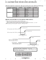
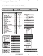
8.5 ADJUSTMENT WHEN THE DRIVE ASSYS ARE REPLACED
TIME LAG ADJUSTMENT OF THE CONTROL SIGNAL (SUS-B)
1
Measure the time lag for the SUS-U signal to the SUS-B signal.
2
Check the time lag for the SUS-B Gate signal to the SUS-U Gate siganl.
Adjust the variable control so that the time lag of Gate becomes " time lag of input
α
±
5 nsec."
Note:
For details on measuring points of waveform, see the figure below.
50 % of the crest value
5 V position
5 V position
Time lag of SUS-U Gate and SUS-B Gate :
Δ
Tsus - gub
Adjust so that "
Δ
Tsus - gub =
Δ
Tsus - iub +
α
±
5 nsec," using the variable
controls shown in the table below:
SUS-U signal (input to the DRIVE Assy)
SUS-B signal (input to the DRIVE Assy)
SUS-U Gate signal
SUS-B Gate signal
X DRIVE (Gate terminal of Q1220)
Y DRIVE (Gate terminal of Q2217)
X DRIVE (Gate terminal of Q1109)
Y DRIVE (Gate terminal of Q2107)
50 % of the crest value
time lag of SUS-U and SUS-B
Δ
Tsus-iub
time lag of SUS-U Gate and SUS-B Gate
Δ
Tsus - gub
Assy
VR
Value of
α
X DRIVE Assy
VR1002
70 nsec
Y DRIVE Assy
VR2002
60 nsec
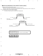
Waveform adjustments required when replacing the following parts of the X DRIVE and Y DRIVE Assys.
Assy Name
Ref No.
Part Name
Part Category
Remarks
X DRIVE Assy
IC1101
PS9117AP
Photo Coupler
IC1104
TND307TD
FET Driver
IC1204
PS9117AP
Photo Coupler
IC1209
TND307TD
FET Driver
Y DRIVE Assy
IC2101
PS9117AP
Photo Coupler
IC2103
TND307TD
FET Driver
IC2104
TND307TD
FET Driver
IC2201
PS9117AP
Photo Coupler
IC2203
TND307TD
FET Driver
Summary of Contents for PDP-5010FD
Page 19: ...PDP 5010FD 19 5 6 7 8 5 6 7 8 C D F A B E ...
Page 20: ...PDP 5010FD 20 1 2 3 4 1 2 3 4 C D F A B E 4 BLOCK DIAGRAM 4 1 OVERALL WIRING DIAGRAM 1 2 ...
Page 23: ...PDP 5010FD 23 5 6 7 8 5 6 7 8 C D F A B E ...
Page 35: ...PDP 5010FD 35 5 6 7 8 5 6 7 8 C D F A B E ...
Page 167: ...PDP 5010FD 167 5 6 7 8 5 6 7 8 C D F A B E ...
Page 178: ...PDP 5010FD 178 1 2 3 4 1 2 3 4 C D F A B E 10 6 PANEL CHASSIS SECTION ...

