PDP-5010FD
123
5
6
7
8
5
6
7
8
C
D
F
A
B
E
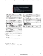
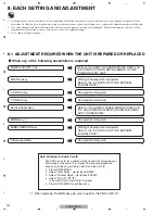
The assembly must be replaced as a unit, and no
part replacement is allowed.
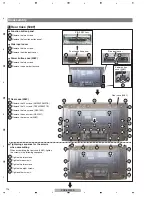
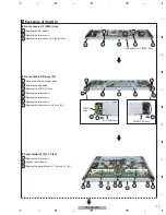
POWER SUPPLY Unit
MAIN Assy
DIGITAL Assy
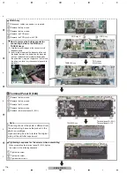
No adjustment is required after replacement of parts
other than those mentioned above.
No adjustment is required after replacement of parts
other than those shown in “8.5 ADJUSTMENTS
WHEN THE DRIVE ASSYS ARE REPLACED.
No adjustment is required after replacement of parts
other than those shown in “8.5 ADJUSTMENTS
WHEN THE DRIVE ASSYS ARE REPLACED.
No adjustment is required after replacement of parts
other than those mentioned above.
No adjustment is required after replacement of parts
other than those mentioned above.
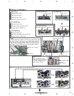
X DRIVE Assy
Y DRIVE Assy
No adjustment required
TANSHI Assy
ADDRESS Assy
No adjustment required
PANEL SENSOR Assy
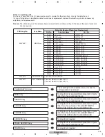
Notes on replacing parts
For the parts described in the list below, replacement is required for the whole Assy, not only the defective part.
If any part listed below is identified as defective and needs replacement, replace the whole Assy, and make necessary
adjustments after replacement.
Reason:
The whole Assy must be replaced, because adjustments and data rewriting for the Assy at the level of production
line are required.
PCB Assy No.
Assy Name
Parts that Require Whole-Assy Replacement
Ref No.
Function Name
Part No.
AWV2457
MAIN Assy
AWV2510
50F X DRIVE Assy • Parts of X D-D CON BLOCK
AWV2511
50F Y DRIVE Assy • Parts of Y MAIN D-D CON BLOCK 1
• Parts of Y MAIN D-D CON BLOCK 2
IC4703
EEPROM
BR24L01AFJ-W
IC4801
MAIN VDEC
CM0048BF
IC4601
AV switch
R2S11006FT
IC4701
RGB switch
R2S11001FT
IC5001
A/D Converter
AD9985KSTZ-110
IC5102
EEPROM
BR24L02FV-W
IC5103
EEPROM
BR24L02FV-W
IC5104
EEPROM
BR24L02FV-W
IC6401
SYSTEM IC
BCM7038KPB1G-B2
IC6602
DDR SDRAM
K4H561638H-UCB3
IC6603
DDR SDRAM
K4H561638H-UCB3
IC6604
DDR SDRAM
K4H561638H-UCB3
IC6605
DDR SDRAM
K4H561638H-UCB3
IC6902
Flash ROM
AGC1057
IC5203
EEPROM
BR24L02FV-W
IC8204
Flash ROM
AGC1049
IC8301
Flash UCOM
AGC1037
IC8602
Flash ROM
AGC1039
Summary of Contents for PDP-5010FD
Page 19: ...PDP 5010FD 19 5 6 7 8 5 6 7 8 C D F A B E ...
Page 20: ...PDP 5010FD 20 1 2 3 4 1 2 3 4 C D F A B E 4 BLOCK DIAGRAM 4 1 OVERALL WIRING DIAGRAM 1 2 ...
Page 23: ...PDP 5010FD 23 5 6 7 8 5 6 7 8 C D F A B E ...
Page 35: ...PDP 5010FD 35 5 6 7 8 5 6 7 8 C D F A B E ...
Page 167: ...PDP 5010FD 167 5 6 7 8 5 6 7 8 C D F A B E ...
Page 178: ...PDP 5010FD 178 1 2 3 4 1 2 3 4 C D F A B E 10 6 PANEL CHASSIS SECTION ...

