Circuit-, IC Descriptions and List of Abbreviations
EN 181
DVDR880-890 /0X1
9.
IC7806
Semiconductor Components Industries, LLC, 2001
August, 2001 – Rev. 9
1
Publication Order Number:
NCP300/D
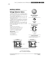
NCP300, NCP301
Voltage Detector Series
The NCP300 and NCP301 series are second generation ultra–low
current voltage detectors. These devices are specifically designed for
use as reset controllers in portable microprocessor based systems
where extended battery life is paramount.
Each series features a highly accurate under voltage detector with
hysteresis which prevents erratic system reset operation as the
comparator threshold is crossed.
The NCP300 series consists of complementary output devices that
are available with either an active high or active low reset output. The
NCP301 series has an open drain N–channel output with either an
active high or active low reset output.
The NCP300 and NCP301 device series are available in the
Thin SOT–23–5 package with seven standard under voltage
thresholds. Additional thresholds that range from 0.9 V to 4.9 V in 100
mV steps can be manufactured.
Features
•
Quiescent Current of 0.5
µ
A Typical
•
High Accuracy Under Voltage Threshold of 2.0%
•
Wide Operating Voltage Range of 0.8 V to 10 V
•
Complementary or Open Drain Reset Output
•
Active Low or Active High Reset Output
Typical Applications
•
Microprocessor Reset Controller
•
Low Battery Detection
•
Power Fail Indicator
•
Battery Backup Detection
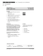
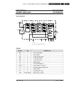
Figure 1. Representative Block Diagrams
This device contains 25 active transistors.
NCP301xSNxxT1
Open Drain Output Configuration
NCP300xSNxxT1
Complementary Output Configuration
V
ref
V
ref
Input
Reset Output
Gnd
3
1
2
Input
Reset Output
Gnd
3
1
2
*
*
* The representative block diagrams depict active low reset output ‘L’ suffix devices. The comparator
inputs are interchanged for the active high output ‘H’ suffix devices.
http://onsemi.com
See detailed ordering and shipping information in the ordering
information section on page 23 of this data sheet.
ORDERING INFORMATION
THIN SOT–23–5
SN SUFFIX
CASE 483
1
5
PIN CONNECTIONS AND
MARKING DIAGRAM
1
3
N.C.
Reset
Output
2
Input
Ground
4
N.C.
5
xxxYW
(Top View)
xxx = 300 or 301
Y
= Year
W
= Work Week
Summary of Contents for DVDR880/001
Page 48: ...Mechanical Instructions EN 50 DVDR880 890 0X1 4 4 5 Dismantling Instructions Figure 4 14 ...
Page 166: ...Circuit IC Descriptions and List of Abbreviations EN 168 DVDR880 890 0X1 9 ...
Page 167: ...Circuit IC Descriptions and List of Abbreviations EN 169 DVDR880 890 0X1 9 ...
Page 174: ...Circuit IC Descriptions and List of Abbreviations EN 176 DVDR880 890 0X1 9 IC7411 ...
Page 182: ...Circuit IC Descriptions and List of Abbreviations EN 184 DVDR880 890 0X1 9 ...
Page 183: ...Circuit IC Descriptions and List of Abbreviations EN 185 DVDR880 890 0X1 9 ...
Page 184: ...Circuit IC Descriptions and List of Abbreviations EN 186 DVDR880 890 0X1 9 ...
Page 203: ...Circuit IC Descriptions and List of Abbreviations EN 205 DVDR880 890 0X1 9 ...

