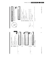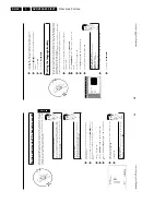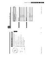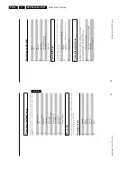
background image

Directions For Use

EN 15

DVDR880-890 /0X1

3.

20

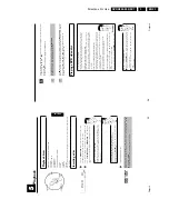
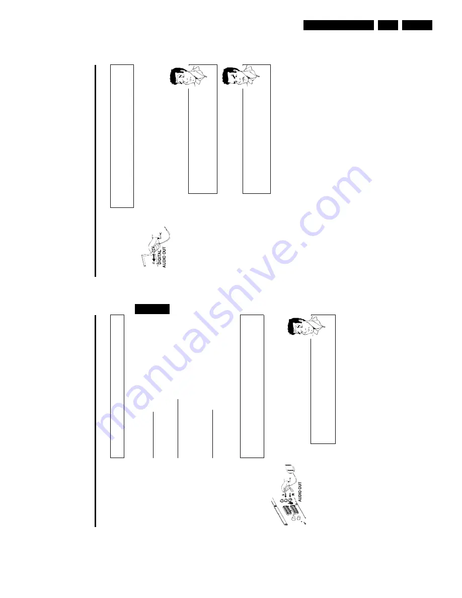
Connecting

audio

devices

to

the

digital

audio

socket

At

the

back

of

the

DVD

recorder

there

is

a

digital

audio

output

socket

DIGITAL

AUDIO

OUT

for

an

coaxial

cable.

These

can

be

used

to

connect

the

following:

•)

an

A/V

receiver

or

an

A/V

amplifier

with

a

digital

multichannel

sound

decoder

•)

a

receiver

with

twochannel

digital

stereo

(PCM)

Digital

multichannel

sound

?

Digital

multi-channel

sound

offers

the

best

possible

sound

quality.

You

will

need

a

multi-channel

A/V

receiver

or

amplifier

that

supports

at

least

one

of

the

audio

formats

of

the

DVD

recorder

(MPEG2,

Dolby

Digital

and

DTS).

Consult

the

operating

instructions

for

your

receiver

to

find

out

which

audio

formats

it

supports.

?

a

All

I

can

hear

from

my

loudspeakers

is

a

loud

distorted

noise

b

The

receiver

is

not

compatible

with

the

digital

audio

format

of

the

DVD

recorder.

The

audio

format

of

the

DVD

disc

is

displayed

in

the

status

window

when

you

switch

to

another

language.

Playback

in

six-channel

digital

surround

sound

is

only

possible

if

the

receiver

has

a

digital

multi-channel

sound

decoder.

Problem

Connecting

the

DVD

recorder

19

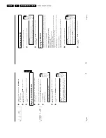
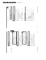
Connect

camcorder

to

the

front

sockets

To

copy

camcorder

recordings,

you

can

use

the

front

sockets.

These

sockets

are

located

behind

the

flap

on

the

left

hand

side.

Best

Picture

Quality

If

you

have

a

DV

or

Digital

8

camcorder,

connect

the

DV

input

of

the

DVD

recorder

to

the

appropriate

DV

output

on

the

camcorder.

Very

good

Picture

Quality

If

you

have

a

Hi8

or

S-VHS(C)

camcorder,

connect

the

S-VIDEO

input

of

the

DVD

recorder

to

the

appropriate

S-VHS

output

on

the

camcorder.

You

must

also

connect

the

audio

input

left

AUDIO

right

on

the

DVD

recorder

to

the

audio

output

on

the

camcorder.

Good

Picture

Quality

If

you

have

a

camcorder

that

only

has

a

single

video

output

(Composite

Video,

CVBS),

connect

the

VIDEO

input

on

the

DVD

recorder

to

the

appropriate

output

on

the

camcorder.

You

must

also

connect

the

audio

input

left

AUDIO

right

on

the

DVD

recorder

to

the

audio

output

on

the

camcorder.

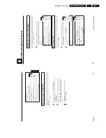
Connecting

audio

devices

to

the

analogue

audio

sockets

Two

analogue

audio

sockets

OUT

L

AUDIO

R

(audio

signal

output

left/right)

are

located

at

the

back

of

the

DVD

recorder.

These

can

be

used

to

connect

the

following:

•)

a

receiver

with

DolbyProLogic

•)

a

receiver

with

twochannel

analogue

stereo

Can

I

use

the

'Phono'

input

on

my

amplifier?

This

socket

(input)

on

the

amplifier

is

designed

only

for

record

players

without

preamplifiers.

Do

not

use

this

input

for

connecting

the

DVD

recorder.

The

DVD

recorder

or

the

amplifier

may

be

damaged

as

a

result.

?

ENGLISH

Connecting

the

DVD

recorder

Summary of Contents for DVDR880/001

Page 1: ...Board In Out Audio IOA Diagram 3 103 Analog Board Power Supply PS Diagram 4 104 Analog Board Multi Sound Processing MSP Diagram 5 105 Analog Board VPS VPS Diagram 6 106 Analog Board Follow Me FOME Diagram 7 106 Analog Board Digital In Out DIGIO Diagram 8 107 Analog Board Audio Converter DAC_ADC Diagram 9 108 UPC 12 Sub PCB Centra Controler CECO Diagram 10 114 UPC 12 Sub PCB Fan Control FACO Diagra...

Page 2: ...rmonic distortion 1 kHz 25 kHz deviation FM 1 5 AM 2 Audio Performance NICAM Frequency response at SCART 1 L R output 40 Hz 15 kHz 0 3dB S N according to DIN 45405 7 1967 and PHILIPS standard test pattern video signal 60 dB unweighted Harmonic distortion 1 kHz 0 5 1 2 7 Tuning Automatic Search Tuning scanning time without antenna typ 3 min PAL stop level vision carrier 37dBµV Maximum tuning error ...

Page 3: ... Outband attenuation 40dB above 30kHz 1 5 2 Scart Audio Output voltage 2 channel mode 1 6Vrms 2dB Channel unbalance 1kHz 1dB Crosstalk 1kHz 85dB Crosstalk 20Hz 20kHz 70dB Frequency response 20Hz 20kHz 0 2dB max Signal to noise ratio 85 dB Dynamic range 1kHz 75dB Dynamic range 20Hz 20kHz 70dB Distortion and noise 1kHz 75dB Distortion and noise 20Hz 20kHz 65dB Intermodulation distortion 70dB Mute sp...

Page 4: ...tance Keep components and tools at this same potential Available ESD protection equipment Complete kit ESD3 small tablemat wristband connection box extension cable and earth cable 4822 310 10671 Wristband tester 4822 344 13999 Be careful during measurements in the live voltage section The primary side of the power supply pos 1005 including the heatsink carries live mains voltage when you connect t...

Page 5: ...ion This product incorporates copyright protection technology that is protected by method claims of certain U S patents and other intellectual property rights owned by Macrovision Corporation and other rights owners Use of this copyright protection technology must be autorized by Macrovision Corporation and is intended for home and other limited viewing uses only unless otherwise authorized by Mac...

Page 6: ...icture on the TV set and playback on the DVD recorder STANDBY m Switch on or off To switch set on or off interrupt menu function interrupt a programmed recording TIMER TV DVD TV DVD switch Switches the scart socket EXT 2 AUX I O directly to the TV set This lets you watch the picture from any unit connected to this scart socket set top box video recorder or satellite receiver and at the same time r...

Page 7: ...ng in progress x A satellite recording has been programmed o A remote control signal has been received k A recording timer has been programmed DECODER A decoder has been assigned to the current TV channel programme RECORD Record Record the current TV channel RECORD LED Recording in progress Red light on the RECORD button to indicate recording in progress OPEN CLOSE Open close disc tray Open close ...

Page 8: ... count BLOCKED It is not possible to close open the disc tray SAFE RECO The new recording will be made at the end of all the other recordings SAFE RECORD EASYLINK The EasyLink function is currently transferring information from the TV set VPS PDC Video programming system programme delivery control A VPS or PDC code will be transmitted for the selected TV program NICAM The DVD recorder has detected...

Page 9: ...n the colour signal and the brightness signal are transmitted on the same cable In certain circumstances this can lead to problems with the picture such as Moiré patterns Connecting the DVD recorder 11 B Connecting the DVD recorder Preparing the remote control for operation The remote control and its batteries are packed separately in the original DVD recorder packaging You must install the batter...

Page 10: ...nnecting with a scart cable without Easy Link Have the following cables ready an aerial cable 1 supplied a mains cable 2 supplied a scart cable 3 1 Remove the aerial cable plug from your TV set Insert it into the ANTENNA socket at the back of the DVD recorder Connecting the DVD recorder 13 Connecting with a scart cable and Easy Link Your DVD recorder can exchange information with your TV set using...

Page 11: ... end of the supplied aerial cable into the TV socket at the back of the DVD recorder and the other end into the aerial input socket at the back of the TV set 3 Plug a scart cable into the scart socket EXT 1 TO TV I O at the back of the DVD recorder and the scart socket for the DVD recorder at the back of the TV set see TV set operating instructions My TV set has several scart sockets Which one sho...

Page 12: ...gh the picture on the TV is fine the recording on a DVD R W is faulty This nterference is unavoidable with copy protected DVDs or video cassettes Problem Connecting the DVD recorder 17 Connecting with video CVBS cable Have the following cables ready an aerial cable 1 supplied a mains cable 2 supplied a video CVBS cable 3 supplied yellow plug an audio cable 4 supplied red white plug 1 Remove the ae...

Page 13: ...dings you can use the front sockets These sockets are located behind the flap on the left hand side Best Picture Quality If you have a DV or Digital 8 camcorder connect the DV input of the DVD recorder to the appropriate DV output on the camcorder Very good Picture Quality If you have a Hi8 or S VHS C camcorder connect the S VIDEO input of the DVD recorder to the appropriate S VHS output on the ca...

Page 14: ...er successfully connecting your DVD recorder to the TV set and other additional devices as described in the previous chapter this chapter will show you how to start the initial installation The DVD recorder automatically seeks out and stores all available TV channels Aim correctly with the remote control In the following sections you will need the remote control for the first time Aim the remote c...

Page 15: ...coder off on the TV screen in the line Decoder using C 0 Confirm with OK A To end press SYSTEM MENU MTV Your decoder has now been allocated to this TV channel When this TV channel is selected the DECODER symbol will appear in the DVD recorder display Installing your DVD recorder 23 Auto Prog Suchl Autom search complete 00 Channels found Time 20 01 Year 2002 Month 01 Date 01 To continue Press OK C ...

Page 16: ...he Follow TV function the information is transferred again from the TV set 1 Switch on the TV set If required select the programme number for the DVD recorder Installing your DVD recorder 25 Manual TV channel search In some cases not all of the available TV channels may have been found and stored during initial installation In this case you will need to search for and store the missing or coded TV...

Page 17: ...7 2 Switch on the DVD recorder using STANDBY ON 3 Press the SYSTEM MENU button on the remote control The menu bar appears 4 Select A using D or C 5 Select Installation using B or A and confirm with C 6 Select Follow TV using B or A and confirm with C 7 Confirm the message on the screen with OK TV 01 will appear in the DVD recorder display TV 01 8 Select programme number 1 on the TV set a I cannot ...

Page 18: ...g and clearing TV channels manually After you have performed the automatic channel search you may not agree with the sequence in which the individual TV channels have been allocated to the programme positions programme numbers You can use this function to rearrange the TV channels already stored or to delete TV channels you don t want or those with poor reception The teletext clock resets automati...

Page 19: ...ast motion L Search by time Information on the TV screen 31 Setting the time and date If the display shows an incorrect time or the time and date must be reset manually If a TV channel which transmits TXT PDC teletext PDC is stored under programme number P01 the time and date will automatically be taken from the TXT PDC information 1 Press SYSTEM MENU on the remote control The menu bar appears 2 S...

Page 20: ...rent time is displayed This box disappears during playback of a disc or after a recording starts f Timer starts on the day shown g OTR recording runs until the stop time displayed h Current time No timer event programmed Information on the TV screen 33 Temporary feedback icons Temporary feedback icons appear in the top left hand corner of the menu bar with information on the different operating mo...

Page 21: ...m the menu b Select the option you want using A B D C or the number keys 0 9 In some cases you need to confirm with OK You can also access the menu using DISC MENU on the remote control Problem How can I access hidden information 1 Press the DISC MENU button on the remote control A menu will appear on the screen For some feature films this may appear after an introductory sequence 2 Select the opt...

Page 22: ...y During playback the current track number and its elapsed playing time will show on the TV screen and on the recorder display During interrupted playback STOP h the current track number will show on the TV screen and on the recorder display If available in the so called ID tag more information will be displayed on album track and artist Tip 2 Stop playback using STOP h The number of albums will b...

Page 23: ...mote control The menu bar will appear at the top of the screen 2 Select the K icon using C or D and confirm with B 3 Using D or C you can now select different speeds forwards or backwards 4 If necessary hide the menu bar using SYSTEM MENU 5 To continue playback press PLAY PAUSE G9 Tip Additional playback features 39 Additional playback features Select the previous or next title with N or O Choose ...

Page 24: ...eatedly until the icons disappear Additional playback features 41 Still picture 1 1 204 1 During playback press PLAY PAUSE G9 to stop the disc and display a still picture Frame by frame playback via menu bar 1 During the still picture press SYSTEM MENU on the remote control The menu bar will appear at the top of the screen 2 Select the I icon using C or D and confirm with B button 3 Using D or C y...

Page 25: ...n using C 2 Select the required subtitle language using B or A You can also enter the number directly using the number buttons 0 9 You can switch off subtitles again with 0 or by pressing off 3 Playback continues in the new subtitle language Additional playback features 43 Scan feature This feature plays back the first 10 seconds of each chapter DVD or track CD 1 During playback press PLAY MODE Se...

Page 26: ...ority CAM2 Digital Video i Link front socket DV Tip Manual recording 45 G Manual recording General information Which discs can I use for recording With th s DVD recorder you can record on two types of DVD DVD RW This disc can be written to and then the contents deleted DVD R This type of d sc can only be recorded once If you want to play this DVD in a DVD player it must be finalized using the Fina...

Page 27: ...EC OTR n button until the message SAFE RECO appears on the display For DVD R discs each new recording is always added at the end of all previous recordings as existing recordings cannot be overwritten On the display will appear e g 5 1 11651 001 Inserting chapter markers During recording it is possible to mark scenes that you want to see or hide later During recording press EDIT at the relevant lo...

Page 28: ... a scart cable and a programming feature Timer For more information please see the operating instructions for the satellite receiver 1 Switch on the TV set If required select the programme number for the DVD recorder 2 Press SYSTEM MENU on the remote control The menu bar appears Manual recording 49 The entire disc is now protected If you try to record onto this disc the message DISC LOCK will appe...

Page 29: ...Recording To switch off the feature select Off using C or D Tip 7 Confirm with OK 8 Use a scart cable to connect the scart socket EXT 2 AUX I O on the DVD recorder to the corresponding scart socket on the satellite receiver 9 Quit using SYSTEM MENU 0 Insert a disc that you want to use for recording A Programme the satellite receiver with the required information programme number of the TV channel ...

Page 30: ...s 3 Select Play full title using A or B and confirm with OK 4 Playback begins automatically The full title including the hidden chapters is played back Managing the disc contents 53 H Managing the disc contents Charly 1 00 29 59 HQ Fri15 02 2002 Empty title 01 30 01 General Information When a recording is made to disc the following additional information is also stored at the beginning of the reco...

Page 31: ...the instructions below 1 Press the STOP h button or during playback press DISC MENU Settings for title Charly 1 Name Charly 1 Play full title Erase this title Press OK 2 Using A or B select the title to be erased and confirm with C The menu for editing titles appears 3 Using A or B select Erase this title and confirm with OK The screen will show This will completely erase this title Press OK to co...

Page 32: ...all markers New index picture Divide ti le Press EDIT to exit How do I select other chapters 1 Press T C on the remote control The title and chapters are shown at the top of the screen 2 Using C or D select Title T or Chapter C 3 Using A or B select the title or chapter you wish to edit Tip 2 Select Current chapter using B Managing the disc contents 57 Finalising DVD R discs This feature is requir...

Page 33: ...divided Managing the disc contents 59 3 Using C select hidden The picture is shown darker Switching quickly You can switch between show chapters visible and hide chapters hidden quickly and easily using SELECT Tip 4 To end press EDIT During playback this chapter will be skipped If the chapter is not visible select visible in step 3 with C Erasing chapter markers You can erase all or some of the ma...

Page 34: ...the time date see Setting the time and date in Installing your DVD recorder a The following message appears on the screen Weekend programming not possible b A daily recording was entered for the wrong day Daily programming can only be used for recordings to be made from Monday to Friday Problem Programming a recording TIMER 61 I Programming a recording TIMER General information Use programmed reco...

Page 35: ...gramming information is stored in a TIMER block 7 To end press TIMER 8 Load a DVD unprotected ready for recording The cassette is being checked 9 Switch off with STANDBY m The programmed recording will only function properly if the DVD recorder has been switched offusing the STANDBY m button If any of the TIMER blocks are in use s will light up on the display Programming a recording TIMER 63 Timer...

Page 36: ...rmation for two programmed recordings overlap b If you ignore this error message the TV programme with the earlier start time will be recorded first You will miss the start of the second programme b Change the information for one of the recordings b Delete one of the recordings Programming a recording TIMER 65 How to check change or delete a programmed recording TIMER 1 Switch on the TV set If req...

Page 37: ...decoder 3D sound The six channels of the digital surround sound Dolby Digital MPEG 2 are mixed down to a two speaker output signal All original audio information is retained The result is an impression of being surrounded by several loudspeakers For TruSurround compatible devices Night mode Night mode optimises the sound for playback at low volume You are therefore less likely to disturb your neig...

Page 38: ...Audio Language Eng ish Subtitle Eng ish Menu Eng ish Country Other Audio Language Playback audio languageAudio Language Subtitle Subtitle language Menu Screen menu language Country Country Additional settings You can select the following functions in this menu Features Access control Enter code Sta us box On Auto resume On Low power standby Off Access control Please read the next chapter Access co...

Page 39: ...recorder 2 Switch on the DVD recorder using STANDBY ON 3 Press SYSTEM MENU The menu bar appears 4 Select the A icon using D or C 5 Select Features using B or A and confirm with C Access control Child Lock 71 K Access control Child Lock Child lock DVD and VCD This feature enables discs to be locked for children When Child Lock is on a 4 digit code PIN needs to be entered before a disc can be played...

Page 40: ...evel using A or B and confirm with C A bar appears to select the parental level 9 Select the appropriate rating using B A or the number buttons 0 9 What do the ratings mean Rating 0 displayed as parental control not active Rating 1 suitable for children Rating 8 only suitable for adults What happens if a DVD scene contains a higher level than the rating set If the recorder does not find a suitable...

Page 41: ...ecording mode HQ with REC MODE during playback from the internal TV tuner MONITOR button This will help achieve the best possible picture quality Before recording select the recording mode as described in chapter Manual Recording section Selecting the recording mode quality b Have your aerial checked b You will find information on how to change the TV system in Manual TV channel search in Installi...

Page 42: ...se observe the following Minimum recording times Recording mode HQ 5 minutes SP 15 minutes EP 20 minutes EP 30 minutes b Some DVD players cannot play back DVD RW recordings You can solve this problem by using a special function You can solve this problem by using a special function 1 Open the disc tray with OPEN CLOSE Insert the disc but do not close the tray 2 Hold down the number button 2 on the...

Page 43: ... DVIO Extender Figure 4 2 DVIO 1 Figure 4 3 DVIO 2 Figure 4 4 4 1 3 Digital board After demounting of DVIO board the top side of the digital board is in reach To reach the bottom side of the digital board the DVDR module must be demounted together with the digital board Connected to each other the assembly can be set in a service position In this position the bottom side of the digital board and t...

Page 44: ...ins inlet of the power supply 2 Remove the screw safety holder 3 Remove the 3 screws of the analog board to the frame 4 Release the snap of the spacer of the analog board to the frame Turn the assembly of the back plate and the analog board against the loader Analog Europe Figure 4 7 Analog NAFTA Figure 4 8 4 1 5 Cable Routing Take care of the correct cable routing See pictures below Europe Figure...

Page 45: ...Mechanical Instructions EN 47 DVDR880 890 0X1 4 4 2 Exploded View of the Set Figure 4 11 TR 01002_001 080502 ...

Page 46: ...Mechanical Instructions EN 48 DVDR880 890 0X1 4 4 3 Exploded View of the complete Front Panel Figure 4 12 TR 01003_001 080502 ...

Page 47: ...Mechanical Instructions EN 49 DVDR880 890 0X1 4 4 4 Exploded View of the Front without PWBs Figure 4 13 TR 01004_001 080502 ...

Page 48: ...Mechanical Instructions EN 50 DVDR880 890 0X1 4 4 5 Dismantling Instructions Figure 4 14 ...

Page 49: ...e microprocessor of the digital board 20 123 HostdI2cNvram checks the data line SDA and the clock line SCL of the I2C bus between the host decoder and NVRAM 19 202 SAA7118I2c checks the interface between the Host I2C controller and the AVENC SAA7118 Video Input Processor 18 200 VideoEncI2c checks the interface between the host I2C controller and Empress SAA6752 17 207 AudioEncI2c checks the I2C co...

Page 50: ...it Press RECORD to indicate that not all labels are lit Press STOP to skip this nucleus 503 4 The local display shows FPLIGHT ALL Press PLAY to start the test Press PLAY to confirm that everything was lit Press RECORD to indicate that not all patterns are lit Press STOP to skip this nucleus 520 5 The local display shows FPLED Press PLAY to start the test Press PLAY to confirm that the led is lit P...

Page 51: ...OUR BAR OFF Press PLAY to start the test Press STOP to skip this nucleus 121 19 The local display shows BERESET Press PLAY to start the test Press STOP to skip this nucleus 603 20 The local display shows BETRAY OPEN Press PLAY to start the test Press STOP to skip this nucleus 616 21 The local display shows BETRAY CLOSE Press PLAY to start the test Press STOP to skip this nucleus 615 22 The local d...

Page 52: ...LAY TO START TEST PRESS ALL KEYS AT LEAST ONCE SEE TABLE FOR KEY CODES PRESS PLAY MORE THAN 1S IF TEST IS OK PRESS RECORD MORE THAN 1S IF TEST IS NOT OK FRONT KEY NAME PLAY STANDBY ON STOP OPEN CLOSE RECORD SEARCH SEARCH CHANNEL DOWN CHANNEL UP FRONT KEY CODE 00E 001 002 003 004 006 005 009 00A LED BECOMES RED PRESS PLAY TO START TEST PRESS AT LEAST ONE KEY ON THE REMOTE CONTROL SEE TABLE FOR RC K...

Page 53: ... execute press STOP to skip press PLAY to execute press STOP to skip press PLAY to execute press NEXT to skip press PLAY to execute press STOP to skip press PLAY to execute press NEXT to skip press PLAY to execute press STOP to skip press PLAY to execute press STOP to skip press STOP to continue DIGITAL BOARD ANALOG BOARD TEST FRONTPANEL TEST PLAY BASIC ENGINE TEST IF ERROR PRESS STOP TO STEP DOWN...

Page 54: ...5 7 The first line indicates that the Diagnostic software has been activated and contains the version number The next lines are the successful result of the SDRAM interconnection test and the basic SDRAM test The last line allows the user to choose between the three possible interface forms If pressing C has made a choice for Command Interface the prompt DD will appear The diagnostic software is n...

Page 55: ...bar 1 White 2 Yellow 3 Light blue 4 Green 5 Magenta 6 Red 7 Blue 8 Black 9 Colour triangle execution time is 12 seconds 10 Test image for progressive scan execution time is 6 seconds b Video standard 0 PAL BDGHI 1 NTSC 136 Video Test Signal Off 137 Macrovision Off xx yy Number Nuclei 200 Video Encoder I2C 202 SAA7118 I2C 203 Audio Encoder SRAM Access 204 Audio Encoder Access 205 Audio Encoder SRAM...

Page 56: ...video and audio signals from the tuner available on Scart2 send command 712 08 For Nafta Apac To make the black white Video available on Y C Rear Out connector send command 712 08 Input 725 frequency in MHz 16 system System NTSC 16 PAL BG 16 PAL I 32 PAL DK 48 SEC L 64 SEC LS 80 SEC BG 96 SEC DK 112 727 Set virgin bit 728 Clear Virgin Bit 729 Write read I2C message to from analogue board xx yy Num...

Page 57: ...ignal from Digital Board is routed to Rear Y C Connector and Input Y c Signal from Front Y C connector is routed to Digital Board PATH ID DESCRIPTION 00 Input signal is VIDEO CVBS from digital board and will be re routed back to the digital board A Cinch Cable need to be connected from Rear Cinch Out to Front Cinch In for this Test Direct routing on analogue board from YUV In to YUV Out is not Pos...

Page 58: ...oard 03 Input Audio Signal is routed from FRONT Cinch In to Digital Board This is same as path id 01 04 Input Signal is from Rear Cinch In1 and it will be routed to Digital Board 05 No routing 06 No routing 07 No routing 08 No Routing 09 No routing 10 No Routing 11 No Routing 12 No Routing 13 Input Signal is from Digital Board and it will be routed to the digital board 14 No routing 15 Input is Au...

Page 59: ...of the SDRAM interconnection test and the basic SDRAM test The last line allows the user to choose between the three possible interface forms If pressing M has made a choice for Menu Interface the Main Menu will appear DVD Video Recorer Diagnostic Software version 48 Basic SDRAM Data bus test passed Basic SDRAM Address bus test passed Basic SDRAM Device test passed M enu C ommand or S 2B interface...

Page 60: ...nu 1 Sine On 2 Sine Burst 1kHz 3 Sine Burst 12kHz VSM Menu 1 Register Access 2 SDRAM Access 3 VSM SDRAM Write Read 4 Interrupt Lines 5 VSM Interconnection 6 UART AVENC Menu 1 Empress 2 Video Input Processors Empress Menu 1 Version number Video Input Processors Menu 1 SAA7118 I2C Access NVRAM Menu 1 Read Error Log 2 Reset Error Log 3 Read DVIO Unique ID Analogue Board Menu 1 Echo 2 Obsolete 3 Route...

Page 61: ... Video Loop 2 System Video Loop VBI 3 System Audio Loop SCART EURO 4 System Audio Loop CINCH NAFTA Basic Engine Loops Menu 1 Basic Engine write read 2 Basic Engine write read endless loop Log Menu 1 Read Error Log 2 Reset Error Log Script Menu 1 User Dealer Script 2 Player Script 5 4 Nuclei Error Codes In the following table the error codes will be described Error Nr Error String 10000 Checksum is...

Page 62: ...re start 20202 SAA7118 VIP access time out 20203 No acknowledge from SAA7118 VIP 20204 No data received from SAA7118 VIP 20300 20301 Error audio encoder SRAM access cannot initial ise I2C 20302 Error audio encoder SRAM access cannot reset DSP through I2C 20303 Error audio encoder SRAM access cannot down load boot 20304 Error audio encoder cannot download test code 20305 Error audio encoder cannot ...

Page 63: ...VSM SDRAM Bank2 Physical memory device test goes wrong 30200 30201 VSM SDRAM Bank1 Memory databus test goes wrong 30202 VSM SDRAM Bank1 Memory addressbus test goes wrong Error Nr Error String 30203 VSM SDRAM Bank1 Physical memory device test goes wrong 30204 VSM SDRAM Bank2 Memory databus test goes wrong 30205 VSM SDRAM Bank2 Memory addressbus test goes wrong 30206 VSM SDRAM Bank2 Physical memory ...

Page 64: ...0803 The frontpanel did not show vertical segments 50804 The user skipped the FP vertical segments test 50805 The user returned an unknown confirmation con firmation 50900 Error Nr Error String 50901 Execution of the command on the analogue board failed 50902 The frontpanel could not be accessed by the ana logue board 50903 The frontpanel did not show horizontal segments 50904 The user skipped the...

Page 65: ...sic Engine to Serial Error Nr Error String 60803 Communication time out error 60804 Unexpected response from Basic Engine 60805 Radial loop could not be closed 60900 60901 Basic Engine returned error number 0xerrornumber 60902 Parity error from Basic Engine to Serial 60903 Communication time out error 60904 Unexpected response from Basic Engine 61500 61501 Basic Engine returned error number 0xerro...

Page 66: ... Error Nr Error String 63100 Number of times Tray went Open Closed nr1 Total hours the CD laser was on nr2 Total hours the DVD laser was on nr3 Total hours the write laser was on nr4 63101 Basic Engine returned error number 0xerrornumber 63102 Parity error from Basic Engine to Serial 63103 Communication time out error 63104 Unexpected response from Basic Engine 63200 63201 Basic Engine returned er...

Page 67: ...the Sound Processor on the Analogue Board fails 70902 Communication with Analogue Board fails 71000 AV Selector test OK Error Nr Error String 71001 Test of the AV Selector on the Analogue Board fails 71002 Communication with Analogue Board fails 71100 NVRAM test OK 71101 Test of the NVRAM on the Analogue Board fails 71102 Communication with Analogue Board fails 71200 Video routing on the Analogue ...

Page 68: ...andleS tateSending 80310 Maximal number of retries NACKs reached HandleStateSending Error Nr Error String 80311 We tried to receive a reply for DVIO_MAX_RETRIES_ACKREPLY times 80312 We tried to receive a reply for DVIO_MAX_RETRIES_REPLY times 80313 We tried to receive an Ack for DVIO_MAX_RETRIES_ACK times 80314 VSM UART error timeout transmitting command 80315 VSM UART error timeout receiving repl...

Page 69: ...AwaitingReply func tion Error Nr Error String 80709 Maximal number of retries reached by HandleS tateSending 80710 Maximal number of retries NACK s reached HandleStateSending 80711 We tried to receive a reply for DVIO_MAX_RETRIES_ACKREPLY times 80712 We tried to receive a reply for DVIO_MAX_RETRIES_REPLY times 80713 We tried to receive an Acknowledge for DVIO_MAX_RETRIES_ACK times 80714 VSM UART e...

Page 70: ... to ENCODING mode 90428 The video encoder could not start from STOP IDLE mode Error Nr Error String 90429 The video encoder did not switch from IDLE to STOP mode 90500 90501 Initialisation of I2C failed 90502 I2C communication to VIP failed 90503 Initialisation of VIP failed 90504 Generation of Close Caption data failed 90505 VIP not locked to video signal 90506 Initialisation of VBI Extractor fai...

Page 71: ...cannot initialise audio VSM out port 90912 Error cannot initialise host decoder audio in 90913 Error loop audio user dealer cannot start audio en coder 90914 Error cannot start VSM audio in DMA port 90915 Error starting the 12kHz audio sine 90916 Error transfer data from audio encoder to VSM 90917 Error cannot start VSM AV out DMA port 90918 Error cannot start VSM AV out port Error Nr Error String...

Page 72: ... to reg 1 of phy Bus_LP Phy 0x22 Could not write 0x55 to reg 1 of phy Bus_LP Phy 0x23 Read incorrect default gapcount from Phy Bus_LP Phy 0x24 Read incorrect updated gapcount from Phy Bus_LP Phy 0x25 Read incorrect gapcount from Phy after reset F117 F173 Phy OptoPR 0x26 Expecting no 1394 connectivity while Phy CNA indicates connection F108 PHY_CNA Bus_PC Phy OptoCNA FPGA 0x27 Expecting 1394 connec...

Page 73: ...for comparison This nucleus tests the components on the audio signal path Host decoder Flex connection between connector 1602 digital board and connector 1900 analogue board DAC Op amp Scart switch IC ADC Audio Encoder VIP VSM Figure 5 10 NUCLEUS 900 AUDIO LOOP DIGITAL VIP STI 5508 VSM EMPRESS DIGITAL BOARD ANALOGUE BOARD GND VIP ICLK 27MHz 7500 7403 7200 7100 TR 01008_001 080502 NUCLEUS 901 AUDIO...

Page 74: ...or testing the components on the video VBI signal path The VIP The VSM The Host Decoder This is done by using the internal test signal source digital board only Remark this test is only successful if nucleus 121 is carried out first Figure 5 12 NUCLEUS 902 DIGITAL VIDEO LOOP VIP STI 5508 VSM EMPRESS DIGITAL BOARD ANALOGUE BOARD STV6618 VIP_ICLK 27MHz 7500 7408 7403 7200 7100 TR 01010_001 080502 NU...

Page 75: ...gnal is routed to the output of the analogue board where it will be looped back by means of an external cable Remark this test is only successful if nucleus 121 is carried out first Figure 5 14 NUCLEUS 904 SYSTEM VIDEO LOOP VIP STI 5508 VSM EMPRESS DIGITAL BOARD ANALOGUE BOARD STV6618 SCART TV EUR CINCH OUT NAFTA SCART AUX EUR CINCH IN NAFTA connector 1947 connector 1947 connector 1601 connector 1...

Page 76: ...al path The VIP The VSM The Host Decoder The signal is routed back internally on the analogue board Remark this test is only successful if nucleus 121 is carried out first Figure 5 16 NUCLEUS 906 VIDEO USER DEALER LOOP VIP STI 5508 VSM EMPRESS DIGITAL BOARD ANALOGUE BOARD STV6618 connector 1947 connector 1947 connector 1601 connector 1601 VIP_ICLK 27MHz 7500 7408 7403 7200 7100 TR 01014_001 080502...

Page 77: ...e video encoder The VSM The host decoder Note This Test is not valid for Nafta in DVDR Lead For Europe the sound will be available on scart 2 5 5 12 Nucleus 911 DVIO Video VIP Nucleus for testing the components on the video signal system path The host decoder The analogue board The VIP On the analogue board the video signal will be routed accord ing to the parameter There it will be looped back ex...

Page 78: ...s to be selected by a parameter Remark Nucleus 704 gives the analog board version Analog board Version Selectable parameter Internal call to nucleus 712 01 1 712 21 11 1 712 21 31 2 712 17 31 3 721 18 31 3 712 19 41 2 712 17 41 3 712 18 41 4 712 19 41 5 712 20 71 4 712 19 ...

Page 79: ...0 FAN 12VDC OPTIONAL INTELLIGENT CONTROL ANALOG BOARD MAINS AC S VIDEO SCART II AUX I O SCARTI TO TV I O CVBS AUDIO DIGITAL DIGITAL PCB ENGINE 7 DATA CONTROL LASER EMI BUS 1933 1932 1 1 2 3 4 5 6 7 2 3 4 5 6 7 8 3V3 3V3 3V3 3V3 GND GND 5V 12V GND GND 5V ION 12Vstby Vgnstby SCL SDA INT POR_DC 5STBY 9 10 11 12 A1 A1 V1 V2 V3 A1 A2 A2 A3 A4 A1 V1 V2 V3 V9 V4 V5 V6 V7 V8 V10 V11 V12 V13 V14 2 1 AFCRI ...

Page 80: ... IPOR Reset INT only Sense 3V3STBY ADC DAC UDA1334BTS UDA1361TS Frontend Video Frontend Audio MSP DataSlicer STV5348 Follow Me EEPROM M24C16 IO Video STV6618 IO Audio HEF IC S Power Supply Front µP TMP87CH74F Display I2C Level Shifter I2C 3 3V I2C 5V AKILL I2C I2C INT IPOR_DC I2C SWITCH 5SW I2C_SW PSS SB1 SFS_TS AFC AGC A_DA T A D_DA T A A_RDY D_RDY IRESET_DIG PWONSW WU WSFI FBIN P50 8SC2 STBY ION...

Page 81: ...6 27 28 29 30 SUR AIRQ CPR TXD GND RXD GND WCLK GND ISDATA0 GND BCLK GND FLAG GND SYNC GND I SDATA1 GND N C GND GND GND GND ARESETN N C GND DLOAD GND V4 2 mm JST KR 3V3 5V GND 4V6 GND 5N GND 12V 1933 8 7 6 5 4 3 2 1 2 1 LED LED 1201 1601 1 mm 6 5 4 3 2 1 7 8 9 0 1 2 3 4 5 6 7 8 9 0 1 2 V_IN GNDD U_ N GNDD Y_IN GNDD C_IN GNDD CVBS_Y_IN GNDD GNDD CVBS_OUT_B GNDD Y_OUT_B GNDD C_OUT_B GNDD R_OUT_B GND...

Page 82: ...mV Div 10us Div A DC 500mV Div 10us Div A DC 500mV Div 10us Div A DC 500mV Div 10us Div A DC 50mV Div 2us Div A DC 50mV Div 5us Div A DC 2V Div 2us Div A DC 100V Div 5us Div A DC 100V Div 2us Div A DC 1V Div 5us Div A DC 500mV Div 10us Div A DC 200mV Div 10us Div D_CVBS F4712 A DC 200mV Div 10us Div A DC 200mV Div 10us Div A DC 200mV Div 10us Div A DC 200mV Div 10us Div A_CVBS I405 D_Y F4714 D_C F...

Page 83: ... DC 500mV Div 500us Div A DC 500mV Div 500us Div F501 F502 A DC 500mV Div 500us Div I014 I032 A DC 500mV Div 500us Div Waveforms Analog Board uPC Sub PWB A DC 1 V Div 500us Div A DC 500mV Div 10us Div A DC 500mV Div 10us Div A DC 1 V Div 20us Div TR 01022_001 140502 Waveforms Analog Board uPC Sub PWB I623 SYNC F843 A_CVBS F8008 I818 ...

Page 84: ...CL 16532145_053 eps 031201 Figure 6 2 2V div AC 10us div 2V div AC 200ns div AD_WCLK AE_WCLK 200mV div AC 20us div R_OUT 200mV div AC 20us div CVBS_OUT 2V div DC 20ms div VSYNC 2V div DC 20ms div HSYNC 200mV div AC 20us div G_OUT 200mV div AC 20us div Y_OUT 200mV div AC 20us div C_OUT 200mV div AC 20us div B_OUT 2V div AC 5us div AD_DATAO AE_DATAO AE_DATAI AD_DATAO AE_DATAO AE_DATAI 2V div AC 250n...

Page 85: ...div AC 10us div DAC A Y 2V div DC 20us div HS_IN Waveforms Digital Board 500mV div AC 10us div Cr signal 2V div DC 10ms div VSOUT 2V div DC 10ms div YUV_IN 2V div DC 10us div HSOUT 2V div DC 20us div Y_OUT Cr_OUT Cb_OUT CL 16532145_055 eps 031201 Figure 6 4 2V div DC 100ns div 2V div DC 20ns div 2V div DC 20ns div 2V div DC 20ns div 2V div DC 50ns div uP_clock Clock 27MHz Clockaudtmp Clock 27M_DV ...

Page 86: ...EN 88 DVDR880 890 0X1 6 Block Diagrams Waveforms Wiring Diagram Test points overview Analog Board TR 01061_001 230502 ...

Page 87: ...Block Diagrams Waveforms Wiring Diagram EN 89 DVDR880 890 0X1 6 Test points overview UPC12 Sub PCB TR 01053_001 140502 ...

Page 88: ... C3 F212 C3 F213 C3 F213 C3 F214 C2 F214 C2 F216 A2 F216 A2 F219 B2 F219 B2 F220 C1 F220 C1 F221 B1 F221 B1 F222 A1 F222 A1 F223 C2 F223 C2 F230 B2 F230 B2 F232 B2 F232 B2 F300 E4 F300 E4 F301 D3 F301 D3 F302 E4 F302 E4 F303 D3 F303 D3 F304 D4 F304 D4 F305 E3 F305 E3 F306 E3 F306 E3 F307 D3 F307 D3 F308 B2 F308 B2 F309 B3 F309 B3 F310 D3 F310 D3 F311 D4 F311 D4 F312 F3 F312 F3 F313 E4 F313 E4 F314...

Page 89: ...V 5V 5V 3V3 3V3 3V3 3V3 3V3 3V3 3V3 3V3 3V3 3V3 3V3 3V3 5V 5V Resetn Resetn_BE Reset_DVIO Resetn_VE Sysclk_VSM_5508 ACC_ACLK_OSC ACC_ACLK_PLL VIP_ICLK Sysclk_ProgScan Sysclk_Empress EMI_PROCCLK AE_DATAO VE_DSn VE_DTACKn Mute HSOUT VSOUT DAC A Y DAC B DAC C Y Cb Cr 3V3 3V3 3V3 HSYNC VSYNC CL 16532145_034 eps 101201 ...

Page 90: ...B4 I515 C5 I516 C5 I517 C5 I518 C4 I519 C5 I520 C4 I521 C4 I522 C4 I523 C4 I524 C4 I525 C5 I526 C5 I527 C5 I528 C4 I529 C5 I530 C5 I531 C5 I532 C5 I533 C4 I535 C5 I536 C4 I537 C5 I538 C4 I540 C5 I543 C5 I551 C5 I552 C4 I553 C4 I555 C4 I600 A5 I601 A5 I602 A5 I603 C5 I604 A5 I605 A5 I606 A5 I607 A5 I608 A5 I609 B5 I610 A5 I611 B5 I612 A5 I613 B5 I614 A5 I615 B5 I616 A5 I617 A5 I618 C4 I619 A5 I621 ...

Page 91: ... 3163 C13 3168 C11 3169 D10 3193 F9 K2 GND not used 3194 F9 4101 A3 4102 B3 5110 D9 5190 F12 5191 F13 5192 F13 5193 H4 6100 I2 7100 B6 7101 A3 7102 B3 7103 H4 3108 I6 3109 C12 3110 C12 3111 H5 3113 E12 3120 H7 3121 H7 3122 G9 3123 G9 3127 G7 OPTION OPTION GND 2150 I9 2168 D11 2169 E10 2190 G11 2191 G11 3100 I3 3101 A3 3102 C3 3103 I3 3104 I3 5VSTBY not used from to Analogboard 3105 H5 3106 H5 3107...

Page 92: ...EN 94 DVDR880 890 0X1 7 Circuit Diagrams and PWB Layouts Layout Display Panel DISP TR 01026_001 150502 TR01027_001 PART 1 TR 01028_001 PART 2 ...

Page 93: ...Circuit Diagrams and PWB Layouts EN 95 DVDR880 890 0X1 7 Layout Display Panel Part 1 Bottom View TR 01027_001 150502 ...

Page 94: ...EN 96 DVDR880 890 0X1 7 Circuit Diagrams and PWB Layouts Layout Display Panel Part 2 Bottom View 150502 TR 01028_001 ...

Page 95: ...5 2206 F3 3201 A5 3202 A6 3206 C5 S CONN 3212 E3 3213 F3 6200 A4 6201 C4 150R 3210 GND_FC C Y CINCH F2106 D8 F2107 D8 F2109 C8 I204 F3 F2101 GND_FC F2105 GND_FC F2107 GND_FC F2109 GND_FC 1M 3207 GND_FC 1K 3206 330p 2205 F2008 DF3A6 8FU 6203 F2103 F2106 1 2 3 4 5 6 GND_FC GND_FC 1912 YKF51 2202 330p DF3A6 8FU 6201 1 GND_FC 3201 1K 2 3 4 5 6 7 8 9 ESD GND 1913 GND_FC 1911 PH S 1 75R 3212 6202 DF3A6 ...

Page 96: ...EN 98 DVDR880 890 0X1 7 Circuit Diagrams and PWB Layouts Layout Front Connector Panel FC TR 01030_001 150502 ...

Page 97: ...B C D A B C CH POWER D 1170 C1 1171 C2 1920 B3 3170 B1 3171 B2 3172 C1 F2001 B3 F2002 B3 F2003 B3 I105 C1 I106 C2 1 2 TEMP_SENSE K1 I105 EVQ 11 1170 4K7 3170 1K 3171 F2002 1171 EVQ 11 1920 DA 1 2 3 F2001 I106 F2003 2322640 3172 TR 01031_001 150502 Layout Key Panel KEY TR 01032_001 150502 ...

Page 98: ...A3 F2103 A3 REC_LED REC I101 A1 I102 A1 1 2 3 1 2 3 A B C A B C 0280 C1 1180 B1 1921 A3 3180 A2 3181 A1 3182 A1 RECLED GND K2 MECHPART 0280 F2101 3181 220R 1 2 3 6180 TLHR4205 I101 DA 1921 3182 220R 3180 47K I102 F2103 F2102 1180 EVQ 11 TR 01033_001 150502 Layout Record Key Panel REC TR 01034_001 150502 ...

Page 99: ...07 2 7V 7710 270R TPS 6 0 MHz 0 SB1 1 2 3 4 5 6 7 8 9 10 11 12 13 14 15 1 2 3 0R 0 7V L 0R 3 1V B C D H I 0005 F2 1701 C7 1702 E7 1703 D7 1704 F14 1705 D2 1706 F14 2713 A3 2719 B5 2720 B4 2721 B5 2722 B9 2723 B8 2724 B10 2725 D3 2727 C8 for PAL I only for MSTD only TDA9817 40 4 ADJUST 1706 0 3731 2V 100K 3744 GND GND 7702 PDTC124EU I723 GND I733 I727 5SW 2725 22p GND GND GND GND 3728 100R 10 8 NC ...

Page 100: ...1 75R I407 GND GND GND GND 1u 2438 I441 GND GND GND 7412 PDTC124EU F499 F4707 GND GND I469 GND GND F5202 6423 BZM55 C12 I434 6415 BZM55 C12 I424 1u 2459 6420 BZM55 C12 I453 5SW 6427 BZM55 C12 GND 28 18 GND GND 0350808190 1940 3 GND I467 3409 75R VGNSTBY I429 GND F5101 GND GND 4402 2442 22u GND GND I485 GND 1u 2427 F5120 47K 3446 I486 I444 I445 470p 3456 3422 820R 2444 I448 I462 12VSTBY 6426 BZM55 ...

Page 101: ...536 2506 1u 1u 2515 GND GND GND GND GND F501 100u 2510 I515 100n 2530 I501 GND GND I511 GND 220R 3520 1n 2520 5VSTBY GND 1u 2507 I505 GND 2517 1n 1K 3526 GND 3538 3K9 1K 3501 GND I518 820R 3530 100n 2521 2523 1n 7509 BC817 25W COL I535 1K 3509 10 11 12 13 14 15 2 3 4 5 6 9 VDD 16 VEE 7 VSS 8 I504 HEF4052BT 7503 1 1u 2513 3522 1u 2501 GND 1n 2527 220R 3524 820R MC33079 7502 A 3 2 1 4 11 GND 4K7 351...

Page 102: ...5 4V6 GNDreg 10R 3331 1304 T4A I352 2 GND GND 3365 3K3 GND 9452A 1931 1 GND 12VSTBY GND GNDHOT I332 F309 6310 STTH302 C2 GND F357 2 1 3 3332 5K62 3Vreg 7305 TL431 GNDHOT 7311 BC847BW I310 I350 F341 6306 1N4006GP 5Vreg ION 5V F339 F300 I345 3V3 12V GND F362 I306 12V 2342 1u F319 F305 5VSTBY F326 3368 3K3 7321 PDTC124EU 5Vreg BC847BW 7310 F323 F306 I333 F325 1N4003 5N 22u 2328 6304 GNDHOT F351 I330 ...

Page 103: ...602 A7 2603 A7 GND 1K 3606 I604 10u 2605 I610 100R 3603 GND 10K 3600 I603 10n 2610 4u7 2612 GND 56p 2607 2609 56p GND I605 5602 10u I624 100n 2606 100R 3612 6600 MCL4148 10u 5601 GND F6002 I623 10n 2604 2611 47u I616 5SW1 8SW 2626 2u2 8SW GND 5SW1 TESTEN 4 TP 7 29 VREF1 25 VREF2 42 VREFTOP XTAL_IN 5 6 XTAL_OUT 3601 100R 21 I2S_DA_OUT 16 15 I2S_WS MONO_IN 43 23 24 28 32 22 RESETQ 40 SC1_IN_L 41 SC1...

Page 104: ...3936 100n 2938 GND 5932 I988 I992 I990 I997 I998 I995 I993 I994 I989 I991 100R 3935 47u 2933 3934 100R 22p 2937 GND 1990 HC 49 U 2936 22p GND 13M875 GND GND GND 100n 2935 A_YCVBS SCLSW SDASW 5SW TR 01040_001 150502 Analog Board Follow Me FOME 3942 E1 3943 E2 3944 E3 3945 E3 3946 E2 3947 E4 3948 A1 3950 A3 3951 B2 3952 B3 3953 B2 3954 C2 7932 B2 7933 B3 7934 A A2 7934 B B4 7934 C C2 7934 D D3 F950 ...

Page 105: ...3581 C2 2586 D3 3 4 I490 C1 I491 D2 I492 D3 I493 B4 E A B from PS D E 1951 A4 2580 A3 2581 A1 2585 C3 GND I491 330R 3582 5VDD 5581 10u PC74HCU04D 1 A 2 Y 2581 100u 7580 B PC74HCU04D A 3 Y 4 7580 A Y 10 7580 F PC74HCU04D A 13 Y 12 PC74HCU04D 7580 E 11 A GND I490 F4102 5580 1 2 3 4 6 75R 3580 6RG GND I487 3 2 GND 2K2 3581 3584 470R YKC21 3416 1951 1 F4103 GND 100n 2580 GND I489 560R 1u 2587 2586 5VD...

Page 106: ...8 5001 GND F0002 GND I020 GND GND GND 6001 MCL4148 22R 3020 2R2 3002 GND GND 100K 3010 I036 2012 100n GND GND GND 2015 100n F006 GND GND GND F007 F011 MP13 1001 125mA 3V3DD 3V3DD 5N F0016 3019 22R GND 3008 1K 100n 2018 F0014 2011 10u I003 F0007 2034 470p 2038 4n7 3V3DD 100n 2009 4K7 3009 GND 4004 3026 47K 100n 2003 GND MCL4148 6003 100n 2014 F0005 2040 4n7 10K 3039 22K 3051 3V3DD I018 F0003 GND I0...

Page 107: ...Circuit Diagrams and PWB Layouts EN 109 DVDR880 890 0X1 7 Layout Analog Board Top View TR 01045_001 150502 ...

Page 108: ...EN 110 DVDR880 890 0X1 7 Circuit Diagrams and PWB Layouts Layout Analog Board Overview Bottom View TR 01046_001 150502 ...

Page 109: ...Circuit Diagrams and PWB Layouts EN 111 DVDR880 890 0X1 7 Layout Analog Board Part 1 Bottom View TR 01047_001 150502 ...

Page 110: ...EN 112 DVDR880 890 0X1 7 Circuit Diagrams and PWB Layouts Layout Analog Board Part 2 Bottom View TR 01048_001 150502 ...

Page 111: ...Circuit Diagrams and PWB Layouts EN 113 DVDR880 890 0X1 7 Test points overview Analog Board TR 01061_001 230502 ...

Page 112: ...8 GNDD 3851 10K 3856 F8607 10K GNDD F833 GNDD 3804 10K 1K 3838 F8402 GNDD GNDD 3V3STBY I816 1K 3833 F844 3815 18K 1 E0 2 E1 3 E2 6 SCL 5 SDA 8 VCC 4 VSS 7 WC GNDD I814 M24C16 7808 F8701 2808 100n 3839 27K GNDD GNDD 10p 2811 I803 100n 2806 F820 10K 3857 I824 I821 F822 F801 5VSTBY F8705 VSS1 46 VSS2 11 W F8403 F8609 DQ3 38 DQ4 40 DQ5 42 DQ6 44 DQ7 30 DQ8 32 DQ9 26 E 28 G 9 10 13 14 15 R B 12 RP 37 V...

Page 113: ...3 3925 C1 3927 D2 3928 B1 3929 D2 6901 D4 7902 B C2 3 4 1 3 B 1 1 4 3916 B3 3917 B1 3919 C1 A C D E A B C D not used not used to CECO 1 6 7 8 4 3917 56K 3 2 1 8 4 7902 B LM358D 5 3928 1K 7902 A LM358D I908 I906 I905 6901 BAV70W 1K 3922 GNDD 6903 BAV70W 82K 3927 10K 3923 GNDD I904 470R 3921 5K6 3920 I907 3916 27K GNDD 12VSTBY 33K 3919 GNDD BZM55 C10 6902 10K 3925 12VSTBY GNDD I903 I909 1K 3929 2911...

Page 114: ...EN 116 DVDR880 890 0X1 7 Circuit Diagrams and PWB Layouts Layout UPC 12 Sub PCB Top View TR 01051_001 140502 Layout UPC 12 Sub PCB Bottom View TR 01052_001 140502 ...

Page 115: ...Circuit Diagrams and PWB Layouts EN 117 DVDR880 890 0X1 7 Tests points overview UPC12 Sub PCB TR 01053_001 140502 ...

Page 116: ... 4n7 310412124452 0002 SM6T 6001 5001 DLW31S 6000 TLMH3100 DLW31S 5000 GND1394 2002 4n7 3000 1M 0003 EARTH SPRING GND1394 5 6 7 8 1 2 3 4 GND 1000 54030 1 2 3 4 5 6 1318141 1001 GND GND1394 2000 1n 2 2001 1n 4n7 2003 5V GND PH S 1002 1 DVIO FRONT BOARD CL 16532095_032 eps 080801 Layout DVIO Front Board CL 16532095_033 eps 080801 0002 C1 0003 A2 1000 C1 1001 B2 1002 C2 2000 B1 2001 B1 2002 B2 2003 ...

Page 117: ...7 5 77 83 89 94 106 112 97 AV1FSYNC 100 AV1READY 118 101 AV1SY 103 AV1SYNC AV1VALID 102 AV2CLK 124 AV2D0 133 AV2D1 134 AV2D2 135 AV2D3 136 AV2D4 139 AV2D5 140 141 AV2D6 AV2D7 142 AV2ENDPCK 123 AV2ERR0 LTLEND 1394MODE 47 AV1CLK 99 AV1D0 108 AV1D1 109 AV1D2 110 AV1D3 111 AV1D4 114 AV1D5 115 AV1D6 116 AV1D7 117 AV1ENDPCK 98 AV1ERR0 96 AV1ERR1 F121 PDI1394 7103 F120 2183 100n F152 2148 100n F124 F199 ...

Page 118: ... RST 11 RXD 16 T0 17 T1 2 T2 31 A15 24 A8 25 A9 43 AD0 42 AD1 41 AD2 40 AD3 39 AD4 38 AD5 37 AD6 36 AD7 33 ALE 5 CEX0 6 CEX1 7 CEX2 8 CEX3 7203 P89C51 26 A10 27 A11 28 A12 29 A13 30 A14 3204 10K 3205 47K 3206 47K F222 F210 F221 100MHZ 5200 F206 F220 3217 5V PRSTn 1K 3216 1K PAD 2 PAD 3 PAD 4 PAD 5 PAD 6 PAD 7 PAD 0 7 PAD 0 7 PA 0 15 PA 0 15 SRAMCE0n SRAMRDn PINT0n PINT1n PALE PWRn PRDn PRSTn PRDn ...

Page 119: ...MHZ 2324 10R 3300 100n 2325 100n 2319 100n 2306 2309 100n 2307 100n 100n 2308 2311 100n 100n 2310 WE_ 2318 100n A8 A9 18 CE_ 5 9 25 I O0 6 I O1 7 I O2 10 I O3 11 I O4 22 I O5 23 I O6 26 I O7 27 OE_ 28 8 24 12 1 A1 2 A10 19 20 A11 A12 21 29 A13 A14 30 31 A15 32 A16 A2 3 A3 4 13 A4 A5 14 15 A6 16 A7 17 7301 CY7C1019BV33 10VC A0 LINK AVREADY 3V3_FPGA CCLK 3V3_FPGA_CONF 3V3_FPGA_CONF DATA 3V3_FPGA_CON...

Page 120: ... 134 VSS21 128 VSS20 122 VSS2 14 VSS19 116 VSS18 110 VSS17 104 VCC3 3 6 36 VCC3 3 5 30 VCC3 3 4 24 VCC3 3 3 18 150 VCC3 3 25 VCC3 3 24 144 VCC3 3 23 138 VCC3 3 22 68 VSS10 62 VSS1 7 VID VS 73 VID RDY 83 VID OE 81 VID HS 75 VID FLD 76 VCC3 3 14 84 VCC3 3 13 78 VCC3 3 12 72 VCC3 3 11 66 VCC3 3 10 60 VCC3 3 1 1 TEST 67 VID D2 58 VID D1 57 VID D0 55 VID CLK1 69 VID CLK0 70 VCC3 3 9 54 VCC3 3 8 48 VCC3...

Page 121: ...01 BCK 1 DATAI 3 DEEM CLKO 9 8 MUTE PLL0 10 SFOR0 11 SFOR1 7 6 SYSCLK PLL1 VDDA 13 VDDD 4 VOL 14 VOR 16 VREF DAC 12 VSSA 7506 UDA1334ATS F504 2 3 4 F520 1501 PH S 1 2511 47u YUV 5 YUV 6 YUV 7 3506 33R PINT0n PINT1n LINK_AVVALID LINK AVFSYNC SRAMCE0n SRAMRDn PINT0n PINT1n PALE PWRn PRDn PRSTn LINK_AVCLK LINK_AVSYNC LINK_AVVALID LINK_AVFSYNC LINK_CSn LINK_INTn LINK_AVREADY DOUT IO1 IO3 IO4 IO10 AUD_...

Page 122: ...5 C2 3116 B1 3117 C2 3118 E2 3119 E2 3120 E2 3121 E2 3122 E2 3123 E2 3124 D2 3125 D2 3126 D2 3127 D2 3128 D2 3130 D2 3131 E2 3132 E2 3133 E1 3134 E1 3136 B2 3137 C2 3138 B2 3139 C2 3140 D1 3141 D1 3147 B1 3148 B1 3164 B2 3165 B2 3166 C3 3171 C1 3172 C1 3173 B2 3174 C1 3176 C1 3177 B2 3178 B2 3179 C2 3180 C2 3188 C1 3189 C1 3190 C1 3191 C2 3192 E2 3193 D1 3197 E2 3198 E2 3199 E2 3201 B5 3202 C5 320...

Page 123: ...Circuit Diagrams and PWB Layouts EN 125 DVDR880 890 0X1 7 Layout DVIO Board Part 1 Top View CL 16532145_19a eps 211101 PART 1 ...

Page 124: ...EN 126 DVDR880 890 0X1 7 Circuit Diagrams and PWB Layouts Layout DVIO Board Part 2 Top View CL 16532145_019b eps 211101 PART 2 ...

Page 125: ...2 C3 F212 C3 F213 C3 F213 C3 F214 C2 F214 C2 F216 A2 F216 A2 F219 B2 F219 B2 F220 C1 F220 C1 F221 B1 F221 B1 F222 A1 F222 A1 F223 C2 F223 C2 F230 B2 F230 B2 F232 B2 F232 B2 F300 E4 F300 E4 F301 D3 F301 D3 F302 E4 F302 E4 F303 D3 F303 D3 F304 D4 F304 D4 F305 E3 F305 E3 F306 E3 F306 E3 F307 D3 F307 D3 F308 B2 F308 B2 F309 B3 F309 B3 F310 D3 F310 D3 F311 D4 F311 D4 F312 F3 F312 F3 F313 E4 F313 E4 F31...

Page 126: ...E DATO 104 106 BE FLAG BE SYNC 105 BE V4 107 BE WCLK 102 CPUINT0 50 CPUINT1 49 D PAR D0 33 D PAR D1 ACC ACLK DAI 160 ACC ACLK DEC 51 ACC ACLK OSC 158 ACC ACLK PLL 159 ACC FID 143 ACC PWM 157 176 AE BCLK AE CS 174 AE DATA 178 AE WCLK 177 7100 SAA7333HL I136 4105 100n 2112 I164 4u7 2127 GNDD I134 I110 2129 68p GND 2 3 1 6 VCC 5 4 7103 NC7SZ58 I124 I162 I176 47p 47R 3110 2141 3123 2K 3127 47R GNDD I1...

Page 127: ...C 127 IRQ0 IRQ1 126 125 IRQ2 NRSS OUT 22 PIO0 0 186 PIO0 1 187 157 CPU DATA14 158 CPU DATA15 143 CPU DATA2 144 CPU DATA3 145 CPU DATA4 146 CPU DATA5 147 CPU DATA6 148 CPU DATA7 151 CPU DATA8 152 CPU DATA9 117 CPU OE CPU PROCLK 118 138 CPU RAS1 130 CPU RW 131 CPU WAIT 34 168 CPU ADR8 169 CPU ADR9 128 CPU BE0 129 CPU BE1 139 CPU CAS0 140 CPU CAS1 135 CPU CE0 134 CPU CE1 133 CPU CE2 132 CPU CE3 141 C...

Page 128: ...310 GNDD GNDD GNDD 100n GNDD 100n 2307 1 2 7 14 3 GNDD 7303 A 74LVC00AD 2304 4u7 GNDD 74LVC00AD 7303 C 9 10 7 14 8 2311 4u7 2303 100n GNDD 2312 100n 2300 100n 4u7 2305 7303 B 74LVC00AD 4 5 7 14 6 I308 RB_ 15 RP_ 12 37 VCC 27 VSS1 46 VSS2 W_ 11 41 DQ13 43 DQ14 DQ15 A 1 45 DQ2 33 35 DQ3 38 DQ4 40 DQ5 42 DQ6 44 DQ7 30 DQ8 32 DQ9 E_ 26 G_ 28 10 13 14 16 A18 9 A19 23 A2 A3 22 A4 21 20 A5 19 A6 18 A7 8 ...

Page 129: ...2 201 SM A3 199 SM A4 198 SM A5 169 SM A6 167 SM A7 164 SM A8 162 SM A9 159 SM CS0 208 SM CS3N 197 SD DQ7 68 SD DQ8 66 SD DQ9 64 SD DQM0 70 SD DQM1 69 SD DQM2 102 SD DQM3 100 SD RASN 75 SD WEN 71 SDA 145 SDATA1 2 SDATA2 6 SM A0 206 SM A1 203 SM A10 160 SM A11 163 SD DQ20 115 SD DQ21 117 SD DQ22 120 SD DQ23 122 SD DQ24 121 SD DQ25 118 SD DQ26 116 SD DQ27 113 SD DQ28 111 SD DQ29 108 SD DQ3 58 SD DQ3...

Page 130: ...GNDD 2536 100n 2534 2545 100n 100n FXO 31FT 7503 2 GND 3 OUT 1 TS 4 VDD 100MHZ 5503 GNDD GNDD 3515 1R 2520 4u7 GNDD GNDD 2538 GNDD 2506 100n GNDD 100n GNDD 4500 2500 1n I510 4u7 2539 GNDD 5506 100MHZ GNDD GNDD GNDD 100n 2537 GNDD GNDD 100n 2503 100n 2532 GNDD GNDD 2528 100n 11 14 7 GNDD 2533 100n 7501 D 74LVC32AD 12 13 I518 100MHZ 5504 2544 100n I512 GNDD GNDD 5509 2501 100n 100n 2514 GNDD 100MHZ ...

Page 131: ...3622 1K 3618 2603 22p GNDD GNDD GNDD GNDD 12u 5601 47p 2621 GNDD 1p 2631 I639 I656 I609 I635 I624 BC847B 7601 2624 22p 3629 180R 5605 12u 1K 3613 GNDD I650 3605 1R 3609 75R 3617 560R GNDD GNDD GNDD I607 5603 12u I608 I625 3603 1K GNDD I622 4602 4600 GNDD 4601 I645 2K2 3638 GNDD GNDD 2629 100n 3604 100R I653 I651 I652 I638 I602 3610 1R GNDD 100n 2620 7603 BC847B I616 I647 AE WCLK 5V_Buffer 5V AD SP...

Page 132: ...06 100R 2726 GNDD 3712 33R GNDD GNDD 100n GNDD 2708 100n 2 7 4K7 3702 C 3 6 4K7 3702 D 4 5 3702 B 4K7 5 I713 4K7 3701 D 4 1 8 100n 2711 33R 2 7 33R 3713 A 4 5 33R 3713 C 3 6 3713 B 2 7 3711 A 33R 1 8 3713 D 33R 3711 C 33R 3 6 33R 3711 B 2715 47u GNDD GNDD GNDD GNDD I710 GNDD GNDD 5700 I709 I712 I711 GNDD 2723 47u 33R 3716 D 4 5 33R 3715 A 1 8 3716 B 2 7 3716 C 33R 3 6 5 33R 3710 B 2 7 33R 3 6 33R ...

Page 133: ...Y 36 DAC B 32 DAC C 27 DV CLKOUT 13 52 29 HSYNC_ SYNC_ RESET 40 38 RSET SCL 30 31 SDA 24 35 CB CR3 48 47 CB CR4 CB CR5 46 45 CB CR6 CB CR7 44 43 CB CR8 CB CR9 42 CLKIN 25 37 COMP 14 CR0 15 CR1 16 CR2 CR3 17 18 CR4 19 CR5 CR6 20 7801 ADV7196A 26 33 ALSB 41 51 CB CR0 CB CR1 50 49 CB CR2 GNDD GNDD GNDD I875 I846 AD8061 7802 3 4 1 5 2 100n 2818 1n 100n 2813 2819 GNDD 7803 A AD8062 3 2 1 8 4 2812 100n ...

Page 134: ...47R 7904 B 74LVC04A 3 7 14 4 MK2703S 7900 4 27M 5 CLK 3 GND 7 S0 6 S1 2 VDD 1 X1 8 X2 I906 47R 3906 1n5 2912 GNDD GNDD GNDD 2914 4u7 2915 100n 14 2 GNDD I916 NCP303 7902 CD 5 3 GND 2 INP 4 1 OUTP 74LVC04A 7904 A 1 7 100MHZ 5904 I903 3916 100K 5 6 14 7 I911 5903 GNDD 7702 B 74LVC86ADB 4 I900 100MHZ 12 14 7 GNDD GNDD 11 10 14 7 7905 F 74HCT14D 13 1901 2 2 74HCT14D 7905 E I909 I901 100MHZ I930 5907 G...

Page 135: ... B1 2824 C3 2829 B1 2834 B1 2837 C3 2903 A2 2904 A2 2907 B3 2908 B2 2909 A2 2912 A1 2914 B3 3100 B3 3101 B3 3102 B3 3103 B2 3104 A4 3105 A4 3106 A3 3107 A2 3108 A3 3109 A3 3110 A3 3117 A3 3118 B1 3119 B2 3120 B3 3121 B3 3122 B3 3123 B3 3124 B3 3125 B2 3126 B3 3127 A3 3128 A3 3129 A3 3130 B3 3131 A4 3132 A4 3133 A4 3134 A4 3135 A4 3136 A3 3137 B2 3138 B2 3200 A4 3202 A3 3203 A5 3204 A4 3208 A3 3209...

Page 136: ...EN 138 DVDR880 890 0X1 7 Circuit Diagrams and PWB Layouts Layout Digital Board Part 1 Top View CL 16532145_32a eps 231101 PART 1 ...

Page 137: ...Circuit Diagrams and PWB Layouts EN 139 DVDR880 890 0X1 7 Layout Digital Board Part 2 Top View CL 16532145_32b eps 231101 PART 2 ...

Page 138: ...B2 3111 B5 3112 B5 3113 B4 3114 B4 3115 A3 3116 A3 3201 B5 3205 B5 3206 B5 3207 B4 3212 B5 3229 A2 3230 A1 3231 A1 3232 A2 3238 A1 3239 A1 3240 A1 3241 A1 3300 B2 3301 B3 3402 B4 3404 A4 3405 B4 3406 A4 3407 A4 3502 C5 3503 C5 3504 C5 3505 C5 3506 C5 3507 C5 3508 C4 3509 C4 3513 C5 3515 C4 3600 B4 3606 A1 3607 A1 3608 A1 3616 A1 3617 A1 3618 A1 3626 A1 3627 A1 3628 A1 3703 C2 3705 B2 3706 B2 3710 ...

Page 139: ...Circuit Diagrams and PWB Layouts EN 141 DVDR880 890 0X1 7 Layout Digital Board Part 1 Bottom View CL 16532145_33a eps 231101 PART 1 ...

Page 140: ...EN 142 DVDR880 890 0X1 7 Circuit Diagrams and PWB Layouts Layout Digital Board Part 2 Bottom View CL 16532145_33b eps 231101 PART 2 ...

Page 141: ...2V 5V 5V 3V3 3V3 3V3 3V3 3V3 3V3 3V3 3V3 3V3 3V3 3V3 3V3 5V 5V Resetn Resetn_BE Reset_DVIO Resetn_VE Sysclk_VSM_5508 ACC_ACLK_OSC ACC_ACLK_PLL VIP_ICLK Sysclk_ProgScan Sysclk_Empress EMI_PROCCLK AE_DATAO VE_DSn VE_DTACKn Mute HSOUT VSOUT DAC A Y DAC B DAC C Y Cb Cr 3V3 3V3 3V3 HSYNC VSYNC CL 16532145_034 eps 101201 ...

Page 142: ... I516 C5 I517 C5 I518 C4 I519 C5 I520 C4 I521 C4 I522 C4 I523 C4 I524 C4 I525 C5 I526 C5 I527 C5 I528 C4 I529 C5 I530 C5 I531 C5 I532 C5 I533 C4 I535 C5 I536 C4 I537 C5 I538 C4 I540 C5 I543 C5 I551 C5 I552 C4 I553 C4 I555 C4 I600 A5 I601 A5 I602 A5 I603 C5 I604 A5 I605 A5 I606 A5 I607 A5 I608 A5 I609 B5 I610 A5 I611 B5 I612 A5 I613 B5 I614 A5 I615 B5 I616 A5 I617 A5 I618 C4 I619 A5 I621 A1 I622 A1...

Page 143: ...t Bad or disturbed TV channel reception PAL AFC adjustment 5711 2 HF AGC adjustment 3724 Service tasks after replacement of IC 7710 Purpose Set amplifier control Symptom if incorrectly set Picture jitter if input level is too low and picture distortion if input level is too high TP ADJ MODE INPUT DC Voltmeter Frequ Generator TUNER 38 9MHz 500mVpp at Tuner 1705 Pin 11 F710 IF out 2 5V 0 1V DISC DIS...

Page 144: ...on is stored with command 715 followed by the slash version as parameter The slash versions used in DVDR880 and DVDR890 are the following DVDR880 00X 63 DVDR880 02X 63 DVDR880 05X 64 DVDR890 00X 61 DVDR890 02X 61 DVDR890 05X 62 DVDR890 69X 81 DVDR890 17X 61 Example DD 715 63 Reset of Slash Version Use command 729 to reset the analogue board to the default setting Procedure Put the set in DSW comma...

Page 145: ...cording to the formula below 35828 YEAR 676 WEEK 26 V N 8788 The figures are fixed YEAR WEEK factory code V N are variable Example 35828 01 676 36 26 22 14 8788 69538 decimal Then we translate the decimal number to a hexadecimal number example 69538 decimal 10FA2 hex 4 Last 5 numbers The last 5 numbers exist out of the Lot and SERIAL number We have to translate the decimal number to the next 5 hex...

Page 146: ...on a small PCB together with the REC Switch and controlled via pin 3 of the microcontroller The POS 7180 is used as a driver for the led 9 2 Microcontroller Sub Board UPC12 SUB PCB 9 2 1 General This small PCB is directly soldered in on top of the Analogue Board It is used with no diversity in all three different basic versions Europe NAFTA and APAC Pal Only the software being loaded into the exte...

Page 147: ... and is increased to 10V when the ambient temperature goes up to approx 35 C The second part of the Op Amp 7902 A prevents dam age of any temperature sensitive part in case the NTC or the wire in between is damaged It acts as a comparator and pulls the BE_FAN signal to 10V As the fan has to be stopped in case the tray of the drive is open this voltage is killed by the CC FAN_OFF signal The double ...

Page 148: ... DAC UDA1334BTS UDA1361TS Frontend Video Frontend Audio MSP DataSlicer STV5348 Follow Me EEPROM M24C16 IO Video STV6618 IO Audio HEF IC S Power Supply Front µP TMP87CH74F Display I2C Level Shifter I2C 3 3V I2C 5V AKILL I2C I2C INT IPOR_DC Blockdiagram Control Lines and Bus Systems I2C SWITCH 5SW I2C_SW PSS SB1 SFS_TS AFC AGC A_DA T A D_DA T A A_RDY D_RDY IRESET_DIG PWONSW WU WSFI FBIN P50 8SC2 STB...

Page 149: ...acitor 2309 through the primary coil of the transformer 5300 pins 7 5 the transistor 7307 and resistors 3321 3352 to ground The positive voltage on pin 7 of the transformer 5300 can be assumed as constant for a switching cycle The current in the primary coil of the transformer 5300 increases linearly A magnetic field representing a certain value of the primary cur rent is formed inside the transfo...

Page 150: ...3710 to ground The switch 7701 and the signal SB1 do this The HF AGC is set using the potentiometer 3724 so that with a sufficiently large antenna input signal 74 dBµV the voltage at the IF output of the tuner 1705 pin 11 is 500 mVpp This setting must be carried out when the audio carrier is switched off The demodulated video signal appears on pin 16 of 7710 The AGC voltage at pin 4 is used to det...

Page 151: ...g Audio Out from dig board AL AR DVAL 3 UDA1360 ADC A_DATA to dig board 1 ARADC ALADC 16 UDA1334 DAC VOR VOL 14 ARDAC ALDAC D_DATA from dig board LH Logic 10 9 LL HL MSB LSB HEF4052 2 5 12 L H L H HH LH LL HL HH 3 4 15 14 11 13 1 6 MSB LSB POS 7503 LH Logic 10 9 LL HL MSB LSB HEF4052 2 5 12 L H L H HH LH LL HL HH 3 4 15 14 11 13 1 6 MSB LSB POS 7501 MSP34XX 2 I2C Control 8 9 12 13 26 27 31 30 37 3...

Page 152: ...om the CC µP and the IPFAIL of the power supply unit Additionally to analog audio the set is also equipped with a digital output via cinch plug 1951 The signal is generated on the dig board and routed via audio interface cable and connector 1900 to the Ana PCB Here the DAOUT line first passes a 6 fold inverter 7580 being used as a driver and for performance reasons noise reduction jitter Afterward...

Page 153: ...OME FOME VPS Sync Sep DigOut5 DigOut4 A_C Fast Blk Slow B k FBIN Fast Blk Slow Blk D_CVBS D_Y A_R A_G A_B Front IN CVBS Y C R Pr COUT_TV COUT_AUX Y CVBSOUT_AUX Y CVBSOUT_TV Y CVBSOUT_REC 6dB 6dB 6dB 6dB 6dB 6dB 21 27 23 25 29 31 33 34 FBOUT_TV B PbOUT_TV G YOUT_TV DigOUT1 DigOUT2 DigOUT3 DigOUT4 DigOUT5 DigOUT6 C_Gate SDA SCL 41 10 13 1 4 43 11 40 17 15 19 7 6 9 35 STV6618 Bo C amp Av C amp Av C a...

Page 154: ...than 2 4V the picture ratio is 4 3 For generation of the appropriate DC voltage on the Y C out rear the WSRO line is controlled via pin 18 of 7408 by the CC µP Pin 18 set to low means 4 3 pin 18 set to high determines 16 9 The control of the switching voltage Pin 8 of Scart 1 is done via 3 level pin nr 2 of the STV6618 7408 and the transistors 7405 7407 7409 A low on pin 2 of 7408 causes around 11...

Page 155: ...Out from dig board AL AR Modulator Rear IN 2 AIN2R AIN1R AIN1L Rear Out 2 AL AR DVAR DVAL AMCO 3 UDA1360 ADC A_DATA to dig board 1 ARADC ALADC Y UV CVBS YC Rear IN 1 NAFTA only Rear Out 1 Y UV CVBS YC MSP34XX 2 I2C Control 8 9 12 13 26 27 31 30 37 38 41 40 Q Peak Det Source select Demodulator DACM_L DACM_R SC1_OUT_L SC1_OUT_R LH Logic 10 9 LL HL MSB LSB HEF4052 2 5 12 L H L H HH LH LL HL HH 3 4 15...

Page 156: ...d inverter 7580 being used as a driver and for performance reasons noise reduction jitter Afterwards a transformer 5580 is necessary to achieve the correct level and also to have a ground isolated floating output before the signal is fed via 3580 to cinch plug 1951 The capacitors POS 2580 2582 2583 perform on the one side an AC coupling between connector and set ground On the other side they are n...

Page 157: ... Sep Mute Mu e Mute 5V 0V G YIN_AUX R Pr CIN_AUX B PbIN_AUX G YIN_ENC R Pr CIN_ENC B Pb IN_ENC FBIN_AUX 37 38 28 42 2 44 14 16 18 YR_IN DENC VFV VFV D_CVBS D_Y D_C D_VR D_YG D_UB D gOUT6 D gOUT1 from CECO CSW SSW to FV MSW to FV CTL2 NJM2285 CTL1 3 NJM2285 PSCAN KILL WSRO to digital board from digital board Video IO NAFTA APAC Overview 14 11 2001 CVBSR_IN A_YG D_Y D_C D_VR YR_OUT YR_OUT CR_OUT CR_...

Page 158: ...et to low means 4 3 pin 18 set to high determines 16 9 During Stand By there is also no loop through of any input to any output performed 9 5 Digital Board 9 5 1 Record Mode Video Part Analog Video input signals CVBS YC and UV RGB for EURO and YUV for USA are routed via the analog board to connector 1601 and sent to IC7500 SAA7118 Video Input Processor Digital video input signals DV_IN_DATA 7 0 ar...

Page 159: ...ocessor on the analog board is sent to the RESET LOGIC circuit IRESET_DIG Low in standby mode IRESET_DIG High the whole system is reset and the Digital board is waked up 9 5 8 I2C Bus Sti5508 is master of the I2C bus The following IC s are controlled by the I2C bus IC7201 NVRAM IC7403 EMPRESS IC7500 VIP IC7700 FLI2200 Video Deinterlacer Line Doubler IC7801 ADV7196 Video Denc 9 5 9 EMI Bus The foll...

Page 160: ...OG BOARD ANALOG BOARD SERVICE INTERFACE POWER SUPPLY 1600 1603 1601 1602 1901 1900 3V3 12V 5V 5V ION 6 8 8 1 ION IRESET_DIG BE_FAN 5 2 VIP_FB 7902 7702 RESET RESET LOGIC 6 2 2 IRESET_DIG RESETn RSTN_BE RSTN_DVIO RESETn_BE RESETn_DVIO 7904 7900 7906 27MHz SYSCLK_EMPRESS SYSCLK_PROGSCAN SYSCLK_VSM_5508 CLOCK BUFFER MK2703S ACC_ACLK_PLL 1 2 8 7 1 4 OSC YUV_IN 7 0 7700 DATA ADDRESS CTRL 7800 7801 7802...

Page 161: ...he de interlacer 4 4 4 progressive video is fed to the Analog Devices ADV71967 MacroVision compliant DENC 7801 The YUV current output of the DENC is fed via a low pass filter to the single supply output opamps AD8061 8062 7802 7803 The analog video is fed via a 7 poled flex to the analog board where the YUV 2FH cinch connectors are located 9 6 Divio Board 9 6 1 Short Description of the Module The ...

Page 162: ... DECODER NW700 FPGA EPLD SRAM ROM AUDIO DAC UDA1334ATS PDI1394 L21 LINK uP BUS LINK DATA LINK CONTROLE 3 1 4 5 2 Isolated domain 1394 INTERFACE DV CODEC AUDIO VIDEO OUTPUT FIFO CONTROL MICROPROCESSOR 9 TRISTATE BUFFER 27 MHz 2 2 2 INPUT LED CLOCKGENAUD CLKAUDTMP CLOCKGENVID CLK27M_CON CLK27M_DV CLOCK27M SYSTEM CLOCK AUD_SDI AUD_SDI AUD_SDI AUD_SDI AUD_SDO AUD_BCLK AUD_WS AUD_BCLK AUD_WS AUD_BCLK A...

Page 163: ...ffer type i e 2 buffers that can hold one whole frame each Reset The FPGA controls the reset signals on the board This has the advantage that it is possible to reset the board both from software and hardware Reset Figure 9 5 The board reset NRESET will reset the whole board and the software reset can reset everything except the microprocessor itself Power on reset is implemented by adding pull ups...

Page 164: ...isters extra data from the DV stream that is not decoded into audio or video can be sent to the digital board using pin TXD of the serial interface This data includes time stamp and some more Audio Video Output The audio I2S data are sent to audio DAC UDA1334 Analog audio left and right signals are connected to the analog board The tristate buffer enables the digital video stream to the Video Inpu...

Page 165: ...Circuit IC Descriptions and List of Abbreviations EN 167 DVDR880 890 0X1 9 9 7 IC s Display Panel 9 7 1 IC7100 ...

Page 166: ...Circuit IC Descriptions and List of Abbreviations EN 168 DVDR880 890 0X1 9 ...

Page 167: ...Circuit IC Descriptions and List of Abbreviations EN 169 DVDR880 890 0X1 9 ...

Page 168: ...meet a wide range of TV applications It is a full band tuner suitable for CCIR systems B G H L L I and I The low IF output impedance is designed for direct drive of a wide variety of SAW filters with sufficient suppression of triple transient In addition it is equipped with 2 two standard items one a 5 level Analog Digital Converter and the other an internal wide band AGC with I 2 C selectable TOP...

Page 169: ...lect SCL 4 I 2 C Bus Serial Clock SDA 5 I 2 C Bus Serial Data n c 6 Not Connected Vs 7 PLL Supply Voltage 5V n c ADC 8 Not Connected ADC Input 1 VST 9 Fixed tuning Supply Voltage 33V n c 10 Do not connect IF1 11 Asymmetrical IF Output GND M1 M2 M3 M4 Mounting Tags Ground Gain controllable Pre amplifiers TV IF o p RF i p AS SDA SCL 33V Pre filtering Tracking filters PLL AGC Detector Mix Osc IF amp ...

Page 170: ...m Clamp on al l CVBS Y Avera ge Clamp on C Input s Bott om Clamp on RGB Sync tip Clamp on PrPb signals Band width 15 MHz Crossta lk 50 dB DESCRIPTION The STV6618 is a highly integrated I C bus controlled video switch matrix optimized for use in recordable Digital Video Disk applications or DVD players It provides video routings required for connections to two external devices Europe 2 SCARTs inter...

Page 171: ...n 5 17 R PR CIN_AUX Red or Pr or Chroma input from Auxiliary SCART2 or external Cinch 18 DIGOUT6 Digital Output Pin 6 19 Y CVBSIN_AUX Y CVBS Input from Auxiliary SCART2 or external Cinch 20 VCCB_REC Video Output Recorder Buffer Supply Pin 21 Y CVBSOUT_REC Y CVBS Output to Recorder 22 GNDB_REC Ground Supply for Recorder Buffer 23 COUT_AUX Chroma Output to Auxiliary SCART2 or external Cinch 24 VCCB1...

Page 172: ...UT1 Digital Output Pin 1 43 CIN_TUN Chroma Input from Tuner 44 DIGOUT2 Digital Output Pin 2 Figure 2 STV6618 Input Output Diagram Pin No Symbol Description SCART1 TV R PR COUT_TV G YOUT_TV B PBOUT_TV FBOUT_TV Y CVBSOUT_TV Y CVBSIN_TV Tuner Y CVBSIN_TUN Encoder R PR CIN_ENC G YIN_ENC B PBIN_ENC CVBSIN_ENC CIN_ENC YIN_ENC Recorder Y CVBS_REC SCART2 R PR CIN_AUX G YIN_AUX B PB_AUX FBIN_AUX Y CVBSIN_A...

Page 173: ...CVBSOUT_TV SCART1 mute 6 dB Y CVBSOUT_AUX SCART2 mute 6 dB R Pr COUT_TV mute 6 dB G YOUT_TV SCART1 SCART1 mute 6 dB B PbOUT_TV SCART1 Y CVBS_TUN Y CVBS_TV Y CVBS_AUX CVBSIN_ENC YIN_ENC CIN_TV CIN_ENC G YIN_ENC G YIN_AUX R Pr CIN_AUX B PbIN_AUX R Pr CIN_ENC B PbIN_ENC FBOUT_TV SCL FBIN_AUX 0v 5v SDA C_GATE I C Bus Bo Clamp Bo Clamp Bo Clamp Bo Clamp Av Clamp Av Clamp Bot sync av Bo Sync Bot sync Bo...

Page 174: ...Circuit IC Descriptions and List of Abbreviations EN 176 DVDR880 890 0X1 9 IC7411 ...

Page 175: ...very low standby levels 1 W On chip start up current source Protection features Safe restart mode for system fault conditions Continuous mode protection by means of demagnetization detection zero switch on current Accurate and adjustable overvoltage protection Short winding protection Undervoltage protection foldback during overload Overtemperature protection Low and adjustable overcurrent protect...

Page 176: ...art M level V CC 1 2 3 GND S1 CTRL FREQUENCY CONTROL VOLTAGE CONTROLLED OSCILLATOR LOGIC LOGIC OVER VOLTAGE PROTECTION OVERPOWER PROTECTION short winding soft start S2 OVER TEMPERATURE PROTECTION S Q R UVLO Q MAXIMUM ON TIME PROTECTION POWER ON RESET 1 VALLEY TEA1507 100 mV clamp DRIVER START UP CURRENT SOURCE 0 75 V 0 5 V 5 I sense 6 DRIVER MGU230 4 DEM 8 DRAIN 7 HVS n c OCP LEB blank I ss 2 5 V ...

Page 177: ...Circuit IC Descriptions and List of Abbreviations EN 179 DVDR880 890 0X1 9 9 9 IC sUPC12 Sub PCB 9 9 1 IC7825 ...

Page 178: ...ral design In the event that any or all SANYO products including technical data services described or contained herein are controlled under any of applicable local export control laws and regulations such products must not be exported without obtaining the export license from the authorities concerned in accordance with the above law No part of this publication may be reproduced or transmitted in ...

Page 179: ...ltage thresholds Additional thresholds that range from 0 9 V to 4 9 V in 100 mV steps can be manufactured Features Quiescent Current of 0 5 µA Typical High Accuracy Under Voltage Threshold of 2 0 Wide Operating Voltage Range of 0 8 V to 10 V Complementary or Open Drain Reset Output Active Low or Active High Reset Output Typical Applications Microprocessor Reset Controller Low Battery Detection Pow...

Page 180: ...tor threshold VDET This sequence of events causes the Reset output to be in the low state for active low devices or in the high state for active high devices After completion of the power interruption Vin will again return to its nominal level and become greater than the VDET The voltage detector has built in hysteresis to prevent erratic reset operation as the comparator threshold is crossed Alth...

Page 181: ... interface to Motorola s DSP56362 used as MPEG Audio Encoder Glueless interface to Philips HDR65 as part of Basic Engine interface including the Sector Processor as also included in the STi5505 Audio Clock Control providing PLL loop and clock lock detection Double Extraction of VBI decoded data from extended CCIR 656 stream Double UART with hardware handshake and 8 byte Rx Tx FIFO Generation of ad...

Page 182: ...Circuit IC Descriptions and List of Abbreviations EN 184 DVDR880 890 0X1 9 ...

Page 183: ...Circuit IC Descriptions and List of Abbreviations EN 185 DVDR880 890 0X1 9 ...

Page 184: ...Circuit IC Descriptions and List of Abbreviations EN 186 DVDR880 890 0X1 9 ...

Page 185: ...nge Adaptive quantization Motion compensated noise filter 1 3 Audio input Audio inputs I2S format or EIAJ format 16 18 or 20 bits master or slave mode at 32 44 1 and 48 kHz Two digital I2S input ports for selection between two digital audio sources Audio clock generation 256 384 fs 48 kHz locked to video frame rate if video is present Sample rate conversion to 48 kHz locked to video frame rate for...

Page 186: ...intended for customers whose application does not require the DDCE function The SAA6752HS gives significant advantages to customers developing digital recording applications Fast time to market and low development resources By adding a simple external video input processor IC audio analog to digital converter and an external SDRAM analog video and audio sources are compressed into high quality MPE...

Page 187: ...G TRANSMISSION SURVEILLANCE CONFERENCING The SAA6752HS can operate as a stand alone device in all above applications The SAA6752HS full features and flexibility allows customers to tailor functionality and performance to specific application requirements All required control settings such as GOP size and bit rate modes can be selected via I2C bus 3 QUICK REFERENCE DATA 4 ORDERING INFORMATION Notes...

Page 188: ...AUDIO COMPRESSION AUDIO INTER VIDEO FRONT END RAM ROM STREAM MULTIPLEXER OUTPUT INTER VIDEO COMPRESSION SAA6752HS SYSTEM CLOCK REFERENCE CLOCK 27 MHz audio clock I 2 C GPIO reset digital I 2 C bus MIPS RAM ROM TAP PI bus video input digital audio input external MPEG boundary scan CPU clock host interrupt output SDRAM 16 bit 16 Mbit or 16 bit 64 Mbit system clock reference STATIC MEM DEBUG ONLY RES...

Page 189: ... input video input signal bit 3 YUV4 16 input video input signal bit 4 YUV5 17 input video input signal bit 5 YUV6 18 input video input signal bit 6 YUV7 19 input video input signal bit 7 MSB VSSP 20 ground pad ground HSYNC 21 input horizontal sync input video with internal pull down resistor VSYNC 22 input vertical sync input video with internal pull down resistor FID 23 input video eld identi ca...

Page 190: ...t 1 VSSP 53 ground pad ground SD_DQ13 54 input output 8 SDRAM data input output bit 13 SD_DQ2 55 input output 8 SDRAM data input output bit 2 SD_DQ12 56 input output 8 SDRAM data input output bit 12 VDDP 57 supply pad ring supply voltage 3 3 V SD_DQ3 58 input output 8 SDRAM data input output bit 3 SD_DQ11 59 input output 8 SDRAM data input output bit 11 SD_DQ4 60 input output 8 SDRAM data input ou...

Page 191: ..._A5 93 output 8 SDRAM address output bit 5 SD_A0 94 output 8 SDRAM address output bit 0 LSB SD_A4 95 output 8 SDRAM address output bit 4 VSSP 96 ground pad ground SD_A1 97 output 8 SDRAM address output bit 1 SD_A3 98 output 8 SDRAM address output bit 3 SD_A2 99 output 8 SDRAM address output bit 2 SD_DQM3 100 output 8 reserved do not connect VDDP 101 supply pad ring supply voltage 3 3 V SD_DQM2 102...

Page 192: ..._A5 93 output 8 SDRAM address output bit 5 SD_A0 94 output 8 SDRAM address output bit 0 LSB SD_A4 95 output 8 SDRAM address output bit 4 VSSP 96 ground pad ground SD_A1 97 output 8 SDRAM address output bit 1 SD_A3 98 output 8 SDRAM address output bit 3 SD_A2 99 output 8 SDRAM address output bit 2 SD_DQM3 100 output 8 reserved do not connect VDDP 101 supply pad ring supply voltage 3 3 V SD_DQM2 102...

Page 193: ...oat or set to HIGH during normal operating with internal pull up resistor note 3 TMS 135 input boundary scan test mode select pin must oat or set to HIGH during normal operating with internal pull up resistor note 3 TCK 136 input boundary scan test clock pin must be set to LOW during normal operating with internal pull up resistor note 3 TDO 137 3 state output 4 boundary scan test data output pin ...

Page 194: ... 164 output 4 reserved do not connect static memory address output bit 7 SM_A12 165 output 4 reserved do not connect static memory address output bit 12 VSSP 166 ground pad ground SM_A6 167 output 4 reserved do not connect static memory address output bit 6 SM_A13 168 output 4 reserved do not connect static memory address output bit 13 SM_A5 169 output 4 reserved do not connect static memory addre...

Page 195: ...static memory data input output bit 1 with internal pull down resistor SM_D14 193 input output 4 reserved do not connect static memory data input output bit 14 with internal pull down resistor SM_D0 194 input output 4 reserved do not connect static memory data input output bit 0 LSB with internal pull down resistor VDDP 195 supply pad ring supply voltage 3 3 V SM_D15 196 input output 4 reserved do...

Page 196: ...ideo decoder and FLI2220 Enhancer and OSD Generator to produce the highest quality video pipeline for premium applications It is also fully compatible with other decoders having a ITU R BT 656 output format Applications Flat panel TV LCD PDP Progressive scan TVs Multimedia front rear projectors Home Theater Scan Converters Multimedia PCs Workstations DCDi is a Faroudja trademark Features Motion ad...

Page 197: ...IFORMAT2 IFORMAT1 IFORMAT0 OFORMAT2 OFORMAT1 OFORMAT0 N P IN OUT VDD33 VSS VDD33 VSS G YOUT9 G YOUT8 G YOUT7 G YOUT6 G YOUT5 G YOUT4 G YOUT3 G YOUT2 G YOUT1 G YOUT0 VDD33 VSS R CrOUT9 R CrOUT8 R CrOUT7 R CrOUT6 R CrOUT5 R CrOUT4 R CrOUT3 R CrOUT2 R CrOUT1 R CrOUT0 VREFO HREFO VDD25 VSS VSYNC CREFO H CSYNCO B CbOUT9 B CbOUT8 B CbOUT7 B CbOUT6 B CbOUT5 B CbOUT4 B CbOUT3 B CbOUT2 B CbOUT1 B CbOUT0 VD...

Page 198: ...r chroma signal input bus The mode is set by the IFORMAT2 0 pins 32 28 This can be overridden by the IFmtOvr bit bit 3 in register 00H allowing this function to be set or changed via the I2C bus Please refer to the description of register 00H for details Bits 6 4 and 3 in register 08H specify the busses used in the multiplexed modes In all cases the signals are sampled on the rising edges of PIXCL...

Page 199: ...the device address of the control bus to be programmed to prevent conflict with the other devices connected to the bus DADDR1 0 allow the device address to be set to any of the following values C0 C1H C2 C3H E0 E1H E2 E3H Please refer to the section Control Bus Operation and Protocol for further information 46 MODE When this pin is set low the control bus will operate in the slave mode allowing th...

Page 200: ... YCLKO prior to the next rising edge of CCLKO in the YUV 4 2 2 mode and on the rising edge of MEMCLKO in the multiplexed YCbCr pseudo D1 mode 116 CCLKO Chroma output sampling clock This clock is derived from PIXCLK and will be at half the frequency of YCLKO In 30 bit 4 2 2 output mode the chroma output signals will change on the falling edge of YCLKO prior to the next rising edge this clock 117 YC...

Page 201: ...8 MEMCLKO SDRAM clock and 2x output sampling clock This clock is derived from PIXCLK and will be at double the frequency of YCLKO This active signal should be connected to the CLK pin s on the SDRAM s When the 10 bit output mode selected the output signals will also change at this clock rate and this should then be used as the output clock 119 WEN SDRAM Write Enable This active low signal should b...

Page 202: ...Circuit IC Descriptions and List of Abbreviations EN 204 DVDR880 890 0X1 9 9 11 IC s Divio Board 9 11 1 IC7404 NW700 ...

Page 203: ...Circuit IC Descriptions and List of Abbreviations EN 205 DVDR880 890 0X1 9 ...

Page 204: ...AE_WCLK_VSM Audio Encoder I2S word clock to VSM ANA_WE Analogue write enable ANA_WE_LV Analogue write enable Low Voltage B_IN_VIP Video blue input to Video Input Processor B_OUT Video blue output from Host Decoder B_OUT_B Filtered blue video output BA Bank Address BCLK_CTL_SERVICE Bitclock control Service Interface BE_BCLK Basic Engine I2S bit clock BE_BCLK_VSM Basic Engine I2S bit clock to VSM BE...

Page 205: ... Processor G_OUT Video green output from Host Decoder G_OUT_B Filtered green video output from Host Decoder GNDD Digital Ground HD_M_AD 13 0 Host Decoder SDRAM address bus HD_M_CASN Host Decoder SDRAM column address strobe HD_M_CLK Host Decoder SDRAM clock HD_M_CS0N Host Decoder SDRAM chip select HD_M_DQ 15 0 Host Decoder SDRAM data bus HD_M_DQML Host Decoder SDRAM data mask enable Lower HD_M_DQMU...
Page 206: ...18 Power supply for analog input of VIP VDDE_7118 Power supply digital for peripheral cells of VIP VDDI_7118 Power supply digital for core of VIP VDDX_7118 Power supply for crystal oscillator of VIP VE_DATA 7 0 Video Encoder data Bus VE_DSN Video Encoder Data Strobe VE_DTACKN Video Encoder Data Transfer acknowledge VIP_ERROR Video Input Processor error VIP_FB Video Input Processor Fast Blanking VI...

Page 207: ...UD_SDO_DAC Audio Serial Data Output to DAC IC 7506 AUD_WS_701 Audio Word Select to DV CODEC IC 7404 AUD_WS_OUT Audio Word Select to buffer IC 7505 BUFENN_AUD Buffer Enable Audio BUFENN_VID Buffer Enable Video CCLK Configuration Clock CLK27M 27MHz Clock CLK27M_CON 27MHz Clock to Digital Board CLK27M_DV 27MHz Clock Digital Video Codec CLK27M_OSC 27MHz Clock IC7304 CLOCKGENAUD Clock generator Audio C...

Page 208: ...gital Board UART Communication A_RDY Analog board ready status information to digital board A18 A19 Parallel Address Bus CC Flash ROM and S RAM A8 A17 Parallel Address Bus CC Flash ROM and S RAM AD0 AD7 Parallel Address and Data Bus CC Flash ROM and S RAM AFC Automatic Frequency Control AFEL Audio Frontend Left AFER Audio Frontend Right AGC WSRI Automatic Gain Control for Europe Wide Screen Rear I...

Page 209: ... RAM RECLED Control Signal for REC LED RESET_DIG Reset Line to Digital Board RP_ Inverse Reset line to Flash ROM RSA1 2 Record Selector 1 2 RY BY_ Ready Busy input line from Flash ROM SIF1 Sound intermediate frequency SB1 Secam Band 1 PCB Test entrance SCL I C Bus SCLSW Switched I C Bus SDA I C Bus SDASW Switched I C Bus SFS_TS SAW Filter Select Trap Select STBY Standby Line Flash_Toshiba SYNC Vid...

Page 210: ...1583 10nF 10 50V 0603 f 3100 4822 051 30103 10k 5 0 062W 3101 4822 116 52304 82k 5 0 5W 3102 4822 116 52304 82k 5 0 5W 3103 4822 051 30471 470Ω 5 0 062W 3104 4822 051 30471 470Ω 5 0 062W 3105 4822 051 30331 330Ω 5 0 062W 3106 4822 051 30331 330Ω 5 0 062W 3107 4822 051 30103 10k 5 0 062W 3108 4822 051 30102 1k 5 0 062W 3109 4822 116 52283 4k7 5 0 5W 3110 4822 050 11002 1k 1 0 4W 3111 4822 051 30471...

Page 211: ... 100V 2462 4822 124 11947 10µF 20 16V 2463 4822 124 11947 10µF 20 16V 2464 4822 124 21732 10µF 20 25V 2501 3198 017 41050 0603 10V 1µF COL R 2502 2238 586 59812 0603 50V 100NP80M 2503 2238 586 59812 0603 50V 100NP80M 2504 3198 017 41050 0603 10V 1µF COL R 2505 3198 017 41050 0603 10V 1µF COL R 2506 3198 017 41050 0603 10V 1µF COL R 2507 3198 017 41050 0603 10V 1µF COL R 2508 3198 017 41050 0603 10...

Page 212: ...66 2322 574 10402 VDR 0805 1M A 6V4 MAX 21VR 3467 2322 574 10402 VDR 0805 1M A 6V4 MAX 21VR 3468 2322 574 10402 VDR 0805 1M A 6V4 MAX 21VR 3469 4822 117 13632 100k 1 0603 0 62W 3470 4822 117 13632 100k 1 0603 0 62W 3471 4822 117 13632 100k 1 0603 0 62W 3472 4822 117 13632 100k 1 0603 0 62W 3473 4822 051 30101 100Ω 5 0 062W 3474 4822 051 30101 100Ω 5 0 062W 3475 4822 051 30101 100Ω 5 0 062W 3476 48...

Page 213: ... PHSE L 7314h 9965 000 09548 PHOTOCOUPLER TCET1108G VISHAY 7315 4822 209 14933 TL431IZ 7317 9322 163 75685 FET SIG SM SI2306DS VISH 7318 9322 163 75685 FET SIG SM SI2306DS VISH 7319 5322 130 60159 BC846B 7320 9322 163 75685 FET SIG SM SI2306DS VISH 7321 4822 130 61553 DTC124EU 7322 3198 010 42320 BC857BW 7401 3198 010 42320 BC857BW 7402 3198 010 42310 BC847BW 7403 3198 010 42320 BC857BW 7404 3198 ...

Page 214: ...26 11663 12pF 2173 4822 124 23002 10µF 16V 2174 2238 586 59812 0603 50V 100NP80M 2175 4822 124 23002 10µF 16V 2176 2238 586 59812 0603 50V 100NP80M 2177 2238 586 59812 0603 50V 100NP80M 2178 2238 586 59812 0603 50V 100NP80M 2181 4822 124 12095 100µF 20 16V 2182 4822 124 23002 10µF 16V 2183 2238 586 59812 0603 50V 100NP80M 2184 2238 586 59812 0603 50V 100NP80M 2187 2238 586 59812 0603 50V 100NP80M ...

Page 215: ... DVDR890 Various 1000 2422 033 00363 CON BM H 4P F 0 8 B 1001 2422 025 17106 CON BM H 4P F 0 8 IEEE R g 2000 5322 126 10511 1nF 5 50V 2001 5322 126 10511 1nF 5 50V 2002 2020 557 90732 250V 4N7 PM10 R 2002 2222 580 19815 50V 330nF P8020 R 2003 2020 557 90732 250V 4N7 PM10 R 2003 2222 580 19815 50V 330nF P8020 R 2004 2020 557 90732 250V 4N7 PM10 R 2005 2020 557 90732 250V 4N7 PM10 R 2204 2222 867 15...

Page 216: ...NP80M 2619 2238 586 59812 0603 50V 100NP80M 2620 2238 586 59812 0603 50V 100NP80M 2621 4822 126 11785 0603 50V 47P PM5 2622 4822 126 11785 0603 50V 47P PM5 2625 2238 586 59812 0603 50V 100NP80M 2626 4822 126 11785 0603 50V 47P PM5 2627 4822 126 11785 0603 50V 47P PM5 2628 2238 586 59812 0603 50V 100NP80M 2629 2238 586 59812 0603 50V 100NP80M 2630 3198 030 74780 EL SM 35V 4U7 PM20 COL R 2632 2238 5...

Page 217: ...BLM11P600SPT 5204 4822 157 11499 BLM11P600SPT 5205 4822 157 11499 BLM11P600SPT 5207 4822 157 11499 BLM11P600SPT 5208 4822 157 11499 BLM11P600SPT 5209 4822 157 11499 BLM11P600SPT 5300 4822 157 11499 BLM11P600SPT 5302 4822 157 11499 BLM11P600SPT 5400 4822 157 11499 BLM11P600SPT 5402 4822 157 11499 BLM11P600SPT 5403 4822 157 11499 BLM11P600SPT 5404 4822 157 11499 BLM11P600SPT 5500 4822 157 11499 BLM1...

Reviews: