Circuit-, IC Descriptions and List of Abbreviations
EN 160
DVDR880-890 /0X1
9.
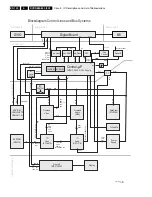
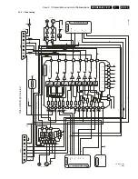
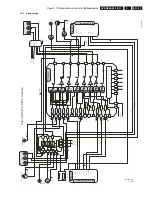
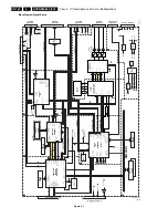
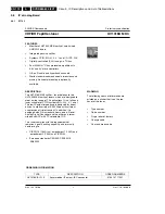
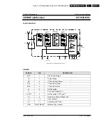
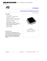
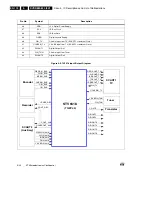
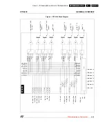
The complete Video-I/O-switching is basically realized by the
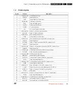
matrix switch STV6618 [7408], which is controlled via I²C-bus
by the CC. All used outputs excluding pin 21 (Y/CVBS-REC)
have a 6dB-amplification and a 75 Ohms-driver-stage inside.
This IC also includes several digital outputs, which are used for
switching purposes on the analog board. The record selector
inside the switch selects between the CVBS from frontend, the
CVBS from Cinch-Rear or Y from the S-Video-input rear.
Afterwards the signal passes another switch [7411] in which a
selection between signals from the front or the preselected
ones is done. The output signals of [7411] are fed as
“A_YCVBS”- and “A_C”-line to the digital board for further
processing.
To reduce the number of external presets there is only one
station for CVBS or Y/C (front and rear). The set automatically
detects between the two inputs depending on the presence of
a video signal (sync separator-circuit on mP-sub-board) where
Y/C has higher priority.
The Y/U/V-inputs are directly routed to the digital PCB. Only
the Y-line has to be present additionally on pin 4 of [7408] for
video recognition.
The signals “D_C” and “D_Y” are fed through [7408] (6dB
amplification) and via [7406], [7409] used as driver to the S-
Video output connector. The “D_CVBS” line is directly routed to
the modulator and via the circuit around [7431] and [7432]
amplified by 6dB before it is fed to the CVBS output plug.
The Y/U/V signals from the digital board are also passing
[7408] for 6dB amplification and driving purpose.
To achieve optimal picture quality the set is equipped with a
simple progressive scan function based on a so-called line
doubler. The complete generation of the signal is done on the
digital board and via a separate cable and connector [1946] the
corresponding Y/U/V lines are routed to the analog PCB. As
there is only one Y/U/V output available a switching between
interlaced and progressive output is necessary. While the
transistors [7421], [7422], [7424], [7425], [7427] and [7428] are
used as driver for Y/U/V progressive, [7423], [7426] and [7429]
together with [7405] are necessary for killing these signals via
pin 42 of [7408] in case the interlaced is selected
(“PSCAN_KILL”-line set to low). If progressive output is active
the pins 27, 29 and 31 of [7408] are set to high impedance and
“PSCAN_KILL” is also high (e.g. 5V).
The detection of the picture ratio information on the Y/C inputs
(rear or front) is done by measuring the DC-level on the
Chroma signal via an analog input of the CC-µP (“WSRI”- and
“WSFI”-line). In case the level is higher than 3,5V the input
signal is a 16:9 source, if the level is lower than 2,4V the picture
ratio is 4:3.
For generation of the appropriate DC-voltage on the Y/C output
the “WSRO”-line is controlled via pin18 of [7408] by the CC-µP
(Pin 18 set to low means 4:3, pin 18 set to high determines
16:9).
During Stand-By there is also no loop-through of any input to
any output performed.
9.5
Digital Board
9.5.1
Record Mode
Video Part
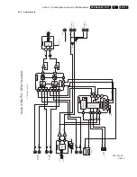
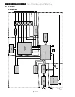
Analog Video input signals CVBS, YC and UV(RGB for EURO
and YUV for USA) are routed via the analog board to connector
1601 and sent to IC7500 SAA7118 (Video Input Processor).
Digital video input signals (DV_IN_DATA(7:0)) are sent from
the DIVIO board through the connector 1603 and further also
to IC7500.
IC7500 (VIP) encodes the analog video to digital video and
processes the digital video to a digital video stream (CCIR656
format). This output stream (VIP_YUV[7:0]) goes to IC7403
SAA6752H (EMPRESS) and to IC7100 Versatile Stream
Manager. The latter uses the data for VBI (vertical blanking
interval) extraction.
IC7403 (EMPRESS) encodes the digital video stream into a
MPEG2 video stream that is fed to IC7100 (VSM).
Audio Part
I2S audio are sent from the analog board to IC7403 EMPRESS
via connector 1602. The EMPRESS compresses I2S audio
data into an AC3 audio stream which is fed to IC7100 (VSM).
Front-End I2S
IC7100 (VSM) interfaces directly to the different hardware
modules such as Basic Engine, EMPRESS IC7403, MPEG
decoder IC7200 (Sti5508) and buffers the data streams that
are coming from or going to these hardware modules.
In IC7100 (VSM), the video MPEG2 stream and the audio AC3
stream are multiplexed into a I2S packetized stream. The serial
data are sent to the Basic Engine to be recorded.
Loop-Through
The multiplexed audio and video stream in the VSM is fed back
via the parallel front-end interface to IC7200 (Sti5508). This IC
decodes the MPEG stream into analog video and I2S audio.
The video and audio signals are routed to the analog board via
connectors 1601 and 1602. During recording, the recorded
signal is present at the outputs of the analog board.
9.5.2
Playback Mode
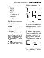
During playback, the serial data from the Basic Engine is going
directly to the Sti5505 via the serial front-end I2S interface.
The Sti5508 is a MPEG & Audio/video decoder and has the
following outputs:
•
To the analog board:
–
analog video RGB, YC, CVBS
–
I2S audio (PCM format)
–
SPDIF audio (digital audio output)
•
To the Progressive scan board:
–
digital video YC(7:0).
9.5.3
S2B Interface
The S2B interface between the VSM (IC7100) and the Servo
processor MACE3 controls the Basic Engine during record and
playback mode.
9.5.4
System Clock
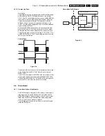
System clocks(27MHz) of VSM, Sti5508, EMPRESS and
Progressive Scan are generated by oscillator 7906
9.5.5
Audio Clock
During record mode, the audio clock ACC_ACLK_OSC is
generated by IC7102 (PLL) because then, the audio clock must
be sychronized with the incoming video (VIP_FID) from the
VIP.
During playback mode, the audio clock ACC_ACLK_PLL is
generated by the clock synthesizer IC7900 (MK2703S).
Both ACC_ACLK_OSC(also goes to the EMPRESS as
ACLK_EMP) and ACC_ACLK_PLL are fed to the VSM. This IC
selects the appropriate clock to the STI5508. The EMPRESS
IC derives from the incoming ACLK_EMP the I2S audio
encoder clocks AE_BCLK and AE_WCLK which are sent to the
VSM.
Summary of Contents for DVDR880/001
Page 48: ...Mechanical Instructions EN 50 DVDR880 890 0X1 4 4 5 Dismantling Instructions Figure 4 14 ...
Page 166: ...Circuit IC Descriptions and List of Abbreviations EN 168 DVDR880 890 0X1 9 ...
Page 167: ...Circuit IC Descriptions and List of Abbreviations EN 169 DVDR880 890 0X1 9 ...
Page 174: ...Circuit IC Descriptions and List of Abbreviations EN 176 DVDR880 890 0X1 9 IC7411 ...
Page 182: ...Circuit IC Descriptions and List of Abbreviations EN 184 DVDR880 890 0X1 9 ...
Page 183: ...Circuit IC Descriptions and List of Abbreviations EN 185 DVDR880 890 0X1 9 ...
Page 184: ...Circuit IC Descriptions and List of Abbreviations EN 186 DVDR880 890 0X1 9 ...
Page 203: ...Circuit IC Descriptions and List of Abbreviations EN 205 DVDR880 890 0X1 9 ...

