OEM628 Technical Specifications
Appendix D
OEM6 Family Installation and Operation User Manual Rev 12
154
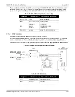
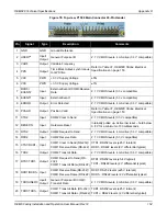
Figure 78: Top-view, P1500 Main Connector 24-Pin Header
Pin
Signal
Type
Description
Comments
1
GND
GND
Ground Reference
–
2
USER1
a
Input/
Output
General Purpose I/O
2.7 V CMOS levels, 4 mA drive (3.3 V compatible)
3
VARF
Output
Variable Frequency
Refer to
Table 31, OEM628 Strobe Electrical
4
PPS
Output
Time Mark Output, synchronous
to GPS time
5
VCC
PWR
+3.3 V Supply Voltage
±5%
6
VCC
PWR
+3.3 V Supply Voltage
±5%
7
RXD3/
EVENT2
Input
External Event 2/COM3 Receive
Data
2.7 V CMOS levels (3.3 v compatible)
8
EVENT1
Input
External Event 1
2.7 V CMOS levels (3.3 v compatible)
9
ERROR
Output
Error Detected
2.7 V CMOS levels, 4 mA drive (3.3 V compatible)
10 PVALID
Output
Position Valid
Refer to
Table 31, OEM628 Strobe Electrical
11 CTS2
Input
COM2 Clear to Send
2.7 V CMOS levels (3.3 V compatible)
12 RESETIN
Input
Hardware Reset
Internally pulled up. Active low reset – hold below
0.8 V for a minimum of 50 milliseconds
13 RTS2
Output
COM2 Request to Send
2.7 V CMOS levels, 4 mA drive (3.3 V compatible)
14 RXD2
Input
COM2 Receive Data
2.7 V CMOS levels (3.3 V compatible)
15 CTS1/RXD1- Input
COM1 Clear to Send (RS-232)/
COM1 Receive Data- (RS-422)
CTS1: RS232 levels (±25 V tolerant)
RXD1-: RS422 levels (2 V differential typical)
16 TXD2
Output
COM2 Transmit Data
2.7 V CMOS levels, 4 mA drive (3.3 V compatible)
17 RTS1/TXD1- Output
COM1 Request to Send (RS-
232)/
COM1 Transmit Data- (RS-422)
RTS1: RS232 levels (±5.4 V typical)
TXD1-: RS422 levels (2 V differential typical)
18 RXD1/RXD1+ Input
COM1 Receive Data (RS-232)/
COM1 Receive Data+ (RS-422)
RXD1: RS232 levels (±25 V tolerant)
RXD1+: RS422 levels (2 V differential typical)
19 TXD3/USER0
Input/
Output
General Purpose I/O/COM3
Transmit Data
2.7 V CMOS levels, 4 mA drive (3.3 V compatible)
20 TXD1/TXD1+ Output
COM1 Transmit Data (RS-232)/
COM1 Transmit Data+ (RS-422)
TXD1: RS232 levels (±25 V tolerant)
TXD1+: RS422 levels (2 V differential typical)


