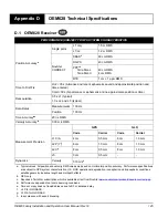
OEM617 Technical Specifications
Appendix B
OEM6 Family Installation and Operation User Manual Rev 12
131
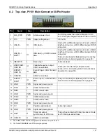
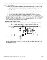
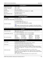
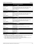
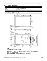
Figure 62: Top-view, P1101 Main Connector 20-Pin Header
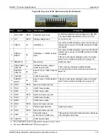
Pin
Signal
Type
Description
Comments
1
LNA_PWR
PWR
Antenna power input
An LDO regulates the output voltage to 5 VDC ±5%.
The input voltage should be 6 VDC to 12 VDC
2
3V3
PWR
Supply voltage input
+3.3 V +5%/-3%
3
USB_D-
IO
USB data (-)
One-half of a differential pair (pins 3 and 4). Match
lengths and route as a 90
Ω
differential pair if USB
is required
4
USB_D+ /
RXD3
a
IO
USB data (+) / COM3 receive
data
One-half of a differential pair (pins 3 and 4). Match
lengths and route as a 90
Ω
differential pair if USB
is required
This pin is internally multiplexed (see
5
/RESETIN
I
Reset input
Active low reset
6
USERVARF /
CAN1RX
IO
Variable frequency output /
CAN1 receive data
These pins are internally multiplexed (see
Connecting Data Communications Equipment
7
EVENT2 /
CAN1TX
IO
Event 2 Input / CAN1 transmit
data
8
CAN2RX
I
CAN2 receive data
9
EVENT1 /
TXD3
a
IO
Event1 input / COM3 transmit
data
This pin is internally multiplexed (see
10 GND
PWR
Signal and power ground
11 TXD1
O
COM1 transmit data
12 RXD1
I
COM1 receive data
13 GND
PWR
Signal and power ground
14 TXD2
O
COM2 transmit data
15 RXD2
I
COM2 receive data
16 GND
PWR
Signal and power ground
17 PV
O
Position valid indicator
Active high output
18 GND
PWR
Signal and power ground
19 PPS
b
O
Timemark output,
synchronous to GPS time
This pin has an internal 50 ohm line driver. Route as
a 50
Ω
single-ended trace
20 CAN2TX
O
CAN2 transmit data
a. The COM3 UART can be configured with firmware on pins 4 and 9.
b. The terms TIMEMARK and PPS are synonymous.

