SUPPORT INFORMATION
M68HC11EVB/D
6-3
3
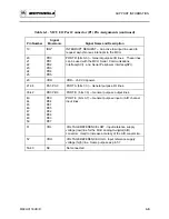
Table 6-1. MCU I/O Port Connector (P1) Pin Assignments (continued)
Pin Number
Signal
Mnemonic
Signal Name and Description
19
IRQ*
INTERRUPT REQUEST
–
An active low input line used to
request asynchronous interrupts to the MCU.
20
21
22
23
24
25
PD0
PD1
PD2
PD3
PD4
PD5
PORT D (bits 0-5)
–
General purpose I/O lines. These lines
can be used with the MCU Serial Communications
Interface(SCI) and Serial Peripheral Interface(SPI).
26
VDD
VDD
–
+5.0 Vdc power.
27-34
PA7-PA0
PORT A (bits 7-0)
–
General purpose I/O lines.
35-42
PB7-PB0
PORT B (bits 7-0)
–
General purpose output lines.
43
44
45
46
47
48
49
50
PE0
PE4
PE1
PE5
PE2
PE6
PE3
PE7
PORT E (bits 0-7)
–
General purpose input or A/D channel
input lines.
51
VRL
VOLTAGE REFERENCE LOW - Input reference supply
voltage (low) line for the MCU analog-to-digital (A/D)
converter. Used to increase accuracy of the A/D conversion.
52
VRH
VOLTAGE REFERENCE HIGH - Input reference supply
voltage (high) line. Same purpose as pin 51.
53-60
NC
Not connected.
Summary of Contents for M68HC11EVB
Page 9: ...CONTENTS x M68HC11EVB D ...
Page 35: ...MONITOR PROGRAM 3 8 M68HC11EVB D ...
Page 81: ...OPERATING INSTRUCTIONS 4 46 M68HC11EVB D ...
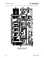
Page 97: ...SUPPORT INFORMATION 6 12 M68HC11EVB D Figure 6 3 EVB Schematic Diagram Sheet 2 of 2 ...
Page 103: ...APPLICATIONS B 2 M68HC11EVB D Figure B 1 Single Chip Mode Configuration ...

