SUPPORT INFORMATION
6-6
M68HC11EVB/D
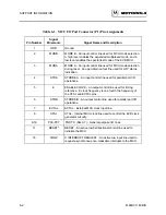
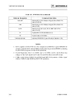
Table 6-4. Input Power Connector (P4) Pin Assignments
Pin Number
Signal
Mnemonic
Signal Name and Description
1
-12 V
-12 Vdc Power - Input voltage (-12 Vdc @ 0.1 A) used by the
EVB logic circuits.
2
GND
GROUND
3
+5 V
+5 Vdc Power - Input voltage (+5 Vdc @ 0.5 A) used by the
EVB logic circuits.
4
+12 V
+12 Vdc Power - Input voltage (+12 Vdc @ 0.1 A) used by the
EVB logic circuits.
Summary of Contents for M68HC11EVB
Page 9: ...CONTENTS x M68HC11EVB D ...
Page 35: ...MONITOR PROGRAM 3 8 M68HC11EVB D ...
Page 81: ...OPERATING INSTRUCTIONS 4 46 M68HC11EVB D ...
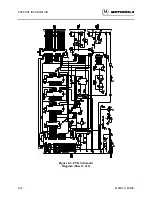
Page 97: ...SUPPORT INFORMATION 6 12 M68HC11EVB D Figure 6 3 EVB Schematic Diagram Sheet 2 of 2 ...
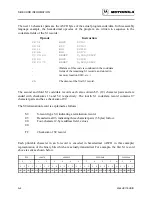
Page 103: ...APPLICATIONS B 2 M68HC11EVB D Figure B 1 Single Chip Mode Configuration ...

