background image

SUPPORT INFORMATION

6-4 

M68HC11EVB/D

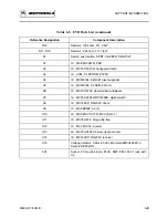
Table 6-2.  Terminal I/O Port Connector (P2) Pin Assignments

Pin Number

Signal

Mnemonic

Signal Name and Description

1

GND

PROTECTIVE GROUND

2

RXD

RECEIVED DATA - Serial data input line.

3

TXD

TRANSMITTED DATA - Serial data output line.

4

NC

Not connected.

5

CTS

CLEAR TO SEND - An output signal used to indicate ready-
to-transfer data status.  This pin is connected to both DSR pin
6 and DCD pin 8.

6

DSR

DATA SET READY - An output signal used to indicate an on-
line/in-service/active status.  This pin is connected to both
CTS pin 5 and DCD pin 8.

7

SIG-GND

SIGNAL GROUND - This line provides signal ground or
common return connection (common ground reference)
between the EVB and RS-232C compatible terminal.

8

DCD

DATA CARRIER DETECT - An output signal used to indicate
an acceptable received line (carrier) signal has been detected.
This pin is connected to both CTS pin 5 and DSR pin 6.

9-19

NC

Not connected.

20

DTR

DATA TERMINAL READY - An input line used to indicate an
on-line/in-service/active status.

21-25

NC

Not connected.

Summary of Contents for M68HC11EVB

Page 1: ...M68HC11EVB D REV 2 November 1996 M68HC11EVB EVALUATION BOARD USER S MANUAL Copyright 1986 1996 by Motorola Inc ...

Page 2: ... reasonable attorney fees arising out of directly or indirectly any claim of personal injury or death associated with such unintended or unauthorized use even if such claim alleges that Motorola was negligent regarding the design or manufacture of the part Information contained in this document applies to REVision C M68HC11EVB Evaluation Boards serial numbers 6000 through 99 999 The computer progr...

Page 3: ...ved when programming or erasing MCU EEPROM locations The EVB MCU configuration CONFIG register ROMON bit is cleared to disable MCU internal ROM thereby allowing external EPROM containing the BUFFALO program to control EVB operations ...

Page 4: ...REPARATION 2 1 2 3 1 Reset Select Header J1 2 2 2 3 2 Clock Select Header J2 2 3 2 3 3 Memory Select Headers J3 and J7 2 4 2 3 4 Program Execution Select Header J4 2 5 2 3 5 Terminal Baud Rate Select Header J5 2 6 2 3 6 Host Port RX Signal Disable Header J6 2 7 2 4 INSTALLATION INSTRUCTIONS 2 7 2 4 1 Power Supply EVB Interconnection 2 7 2 4 2 Terminal EVB Interconnection 2 8 2 4 3 Host Computer EV...

Page 5: ...NS 4 1 INTRODUCTION 4 1 4 2 CONTROL SWITCH 4 1 4 3 LIMITATIONS 4 1 4 4 OPERATING PROCEDURES 4 3 4 4 1 Debugging Mode 4 3 4 4 2 Evaluation Mode 4 3 4 4 3 Monitor Program 4 3 4 5 COMMAND LINE FORMAT 4 4 4 6 MONITOR COMMANDS 4 5 4 6 1 Assembler Disassembler 4 8 4 6 2 Block Fill 4 11 4 6 3 Breakpoint Set 4 12 4 6 4 Bulk 4 14 4 6 5 Bulkall 4 15 4 6 6 Call 4 16 4 6 7 EEPROM Modify Mapping 4 18 4 6 8 Go ...

Page 6: ...Rciser to EVB 4 40 4 8 2 Apple Macintosh with MacTerminal to EVB 4 41 4 8 3 Apple Macintosh with Red Ryder to EVB 4 43 4 8 4 IBM PC with KERMIT to EVB 4 44 4 8 5 IBM PC with PROCOMM to EVB 4 45 CHAPTER 5 HARDWARE DESCRIPTION 5 1 INTRODUCTION 5 1 5 2 GENERAL DESCRIPTION 5 1 5 2 1 Microcomputer 5 1 5 2 2 Port Replacement Unit 5 2 5 2 3 Memory 5 4 5 2 4 Address Decoding De multiplexing 5 4 5 2 5 RS 2...

Page 7: ...FIGURES 1 1 EVB Block Diagram 1 4 2 1 EVB Connector Switch and Jumper Header Location Diagram 2 2 2 2 Terminal Host Computer Cable Assembly Diagram 2 10 2 3 MCU I O Port Extension Cable Assembly Diagram 2 13 5 1 EVB Block Diagram 5 2 5 2 EVB Memory Map Diagram 5 3 6 1 EVB Parts Location Diagram 6 7 6 2 EVB Schematic Diagram Sheet 1 of 2 6 11 6 3 EVB Schematic Diagram Sheet 2 of 2 6 12 B 1 Single C...

Page 8: ...3 3 2 Interrupt Vector Jump Table 3 6 4 1 Monitor Memory Map Limitations 4 2 4 2 Monitor Program Commands 4 6 6 1 MCU I O Port Connector P1 Pin Assignments 6 2 6 2 Terminal I O Port Connector P2 Pin Assignments 6 4 6 3 Host I O Port Connector P3 Pin Assignments 6 5 6 4 Input Power Connector P4 Pin Assignments 6 6 6 5 EVB Parts List 6 8 ...

Page 9: ...CONTENTS x M68HC11EVB D ...

Page 10: ...able of handling a 123K file NOTE Unless otherwise specified all address references are in hexadecimal throughout this manual An asterisk following the signal name denotes that the signal is true or valid when the signal is low 1 2 FEATURES EVB features include An economical means of debugging user assembled code and evaluating target systems incorporating MC68HC11 microcomputer unit MCU device On...

Page 11: ...A1FN PRU MC68HC24FN ACIA MC68B50 I O ports Terminal Host computer MCU extension RS 232C compatible RS 232C compatible HCMOS TTL compatible Temperature Operating Storage 25 degrees C 40 to 85 degrees C Relative humidity 0 to 90 non condensing Power requirements 5 Vdc 0 5 A max 12 Vdc 0 1 A max 12 Vdc 0 1 A max Dimensions Width Length 7 062 in 17 8 cm 4 625 in 11 75 cm ...

Page 12: ...e memory of the MC68HC11 MCU The EVB emulates the single chip mode of operation even though the EVB operates in the expanded multiplexed mode of operation at all times Overall evaluation debugging control of the EVB is provided by the BUFFALO monitor program via terminal interaction The target system interface is provided by the MCU and PRU devices RS 232C terminal host I O port interface circuitr...

Page 13: ...B operation Table 1 2 External Equipment Requirements External Equipment 5 12 12 Vdc power supply 1 Terminal RS 232C compatible Host computer RS 232C compatible 2 Terminal host computer EVB RS 232C cable assembly 1 Target system EVB MCU I O port extension cable assembly 1 1 Refer to Chapter 2 for details 2 Optional not required for basic operation ...

Page 14: ...at the EVB components are properly configured for target system operation The EVB has been factory tested and is shipped with factory installed jumpers Inspect the EVB for jumper placements prior to target system installation Figure 2 1 illustrates the EVB connector switch and jumper header locations Use connector P1 to connect the EVB to the target system Use connectors P2 and P3 to connect the E...

Page 15: ...an external reset signal from the target system via MCU I O port connector P1 pin 17 to be used by the EVB This is accomplished by the installation of a fabricated jumper on pins 1 and 2 The EVB is factory configured and shipped with the jumper installed as shown below J1 1 2 This jumper is removed from pins 1 and 2 when the EVB reset circuitry is used without target system intervention ...

Page 16: ... is an 8 MHz crystal for a bus rate of 2 MHz The EVB is factory configured and shipped with the clock input selected for internal clock source This is accomplished by the installation of a fabricated jumper on pins 2 and 3 as shown below J2 1 2 3 External Internal If an external TTL clock source from the target system via MCU I O port connector P1 pin 7 is required the jumper is repositioned betwe...

Page 17: ... time Jumper header J7 is for factory use only Jumper header J3 or J7 applies a chip enable CE signal to the RAM device installed at location U4 The RAM device is selected or deselected by the installation of a fabricated jumper on either jumper header J3 or J7 If the installed RAM device is not required but left installed both jumper headers J3 and J7 should not have fabricated jumpers installed ...

Page 18: ...nfigured and shipped with the program execution selected for BUFFALO monitor operation as shown below The user must configure the EVB for the type of program execution required If program execution out of EEPROM is desired the jumper is repositioned between pins 2 and 3 J4 1 2 3 Monitor EEPROM 10K PULLDOWN 10K PULLUP If the PE0 line is used for A D operations the loading condition introduced by ju...

Page 19: ...gured and shipped with the terminal baud rate selected for 9600 baud as shown below J5 1 2 3 4 5 6 7 8 9 10 11 12 300 BAUD 600 BAUD 1200 BAUD 2400 BAUD 4800 BAUD 9600 BAUD BAUD RATE SELECTION The host P3 I O port is a fixed MCU SCI 9600 baud rate non selectable Refer to Chapter 6 EVB parts list notes for additional information pertaining to the host baud rate crystal vs E clock vs MCU SCI operatio...

Page 20: ...per installed on pins 1 and 2 2 4 INSTALLATION INSTRUCTIONS The EVB is designed for table top operation A user supplied power supply and RS 232C compatible terminal are required for EVB operation An RS 232C compatible host computer is optional for downloading user assembled code to the EVB 2 4 1 Power Supply EVB Interconnection The EVB requires 5 Vdc 0 5 A 12 Vdc 0 1 A 12 Vdc 0 1 A and GND for ope...

Page 21: ...low The other end of the cable assembly is connected to the user supplied terminal For connector pin assignments and signal descriptions of the EVB terminal port connector P2 refer to Chapter 6 14 15 16 17 18 19 21 22 23 24 25 20 1 2 3 4 5 6 7 8 9 10 11 12 13 NC NC NC NC NC NC DTR NC NC NC NC NC GND RXD TXD NC CTS DSR SIG GND DCD NC NC NC NC NC P2 TERMINAL NOTE A dumb terminal or personal computer...

Page 22: ...host computer For connector pin assignments and signal descriptions of the EVB host port connector P3 refer to Chapter 6 14 15 16 17 18 19 21 22 23 24 25 20 1 2 3 4 5 6 7 8 9 10 11 12 13 NC NC NC NC NC NC DTR NC NC NC NC NC GND RXD TXD NC NC DSR SIG GND DCD NC NC NC NC NC P3 HOST NOTE The RXD and TXD signal directions output versus input are reversed as compared to the terminal I O port The EVB lo...

Page 23: ...CONNECTOR PART S 25 D SUBMINIATURE FEMALE SOCKET CONNECTOR PART S 1 CIRCUIT ASSEMBLY CORP CA 25 SMD P 1 CIRCUIT ASSEMBLY CORP CA 25 SMD S 2 ITT CANNON DBSP B25P 3 ANSLEY 609 25P 4 WINCHESTER 49 1125P 2 ITT CANNON DBSP B25S 3 ANSLEY 609 25S 4 WINCHESTER 49 1125S 20 OR 25 CONDUCTOR FLAT RIBBON CABLE 3M 3365 20 OR 3M 3365 25 Figure 2 2 Terminal Host Computer Cable Assembly Diagram The EVB can operate...

Page 24: ...truct and is illustrated in Figure 2 3 This type of assembly provides an indirect connection of the EVB MCU I O port to the target system MCU device socket Indirect connection is accomplished via a 60 pin connector installed on the target system board that connects to the target system MCU device socket This connector is a double row post 60 pin header type Amptronics 929715 01 30 Target system wi...

Page 25: ...58 60 1 3 5 7 9 11 13 15 17 19 21 23 25 27 29 31 33 35 37 39 41 43 45 47 49 51 53 55 57 59 MODB STRA STRB XTAL PC1 PC3 PC5 PC7 XIRQ PD0 PD2 PD4 Vdd PA6 PA4 PA2 PA0 PB6 PB4 PB2 PB0 PE4 PE5 PE6 PE7 VRH NC NC NC NC GND NC E EXTAL PC0 PC2 PC4 PC6 RESET IRQ PD1 PD3 PD5 PA7 PA5 PA3 PA1 PB7 PB5 PB3 PB1 PE0 PE1 PE2 PE3 VRL NC NC NC NC MCU I O PORT ...

Page 26: ...HARDWARE PREPARATION AND INSTALLATION M68HC11EVB D 2 13 13 Figure 2 3 MCU I O Port Extension Cable Assembly Diagram ...

Page 27: ...in EEPROM MCU U10 If the EVB monitor prompt is not displayed as shown above press the user reset switch S1 If the monitor prompt cannot be displayed the possibility exists that the EVB cannot communicate via the terminal port because the CONFIG register NOSEC bit is enabled logic 0 Erasing the entire EEPROM array including the CONFIG register must be performed as follows 1 Remove installed jumper ...

Page 28: ... The EVB resident MCU have the configuration CONFIG register ROMON bit cleared thereby disabling the MCU internal ROM Having the monitor program in EPROM external to the MCU at locations E000 FFFF is a great advantage because it allows the user to add instructions to customize the monitor for specific requirements The BUFFALO monitor program consists of five parts or sections which are as follows ...

Page 29: ...d ONSCI INSCI and OUTSCI The second set of drivers is for a DUART and these routines are called ONUART INUART and OUTUART The third set of drivers is for an ACIA and these routines are called ONACIA INACIA and OUTACIA All I O communications are controlled by three RAM locations IODEV EXTDEV and HOSTDEV EXTDEV specifies the external device type 0 none 1 ACIA 2 DUART HOSTDEV specifies which I O port...

Page 30: ... table FF82 RPRINT Display user s registers FF85 HEXBIN Convert ASCII character in A register to 4 bit binary number Shift binary number into SHFTREG from the right SHFTREG is a 2 byte 4 hexadecimal digits buffer If A register is not hexadecimal location TMP1 is incremented and SHFTREG is unchanged FF88 BUFFAR Read 4 digit hexadecimal argument from input buffer to SHFTREG FF8B TERMAR Read 4 digit ...

Page 31: ...pointing to next byte FFBE OUT1BS Convert binary byte at address in index register X to two ASCII characters and output followed by a space Returns address in index register X pointing to next byte FFC1 OUT2BS Convert two consecutive binary bytes starting at address in index register X to four ASCII characters and output followed by a space Returns address in index register X pointing to next byte...

Page 32: ...cond entry is the ASCII command name The third entry is the starting address of the command module As an example FCB 3 3 characters in command name FCC ASM ASCII literal command name string FDB ASM Jump address for command module Each command in the BUFFALO program is a individual module Thus to add or delete commands all that is required is to include a new command module or delete an existing mo...

Page 33: ...2 00E4 Timer Input Capture 2 00E5 00E7 Timer Input Capture 1 00E8 00EA Real Time Interrupt 00EB 00ED IRQ 00EE 00F0 XIRQ 00F1 00F3 Software Interrupt SWI 00F4 00F6 Illegal Opcode 00F7 00F9 Computer Operating Properly COP 00FA 00FC Clock Monitor 00FD 00FF To use vectors specified in Table 3 2 the user must insert a jump extended opcode in the three byte field of the vector required For an example fo...

Page 34: ...terrupt vectors which would cause undesirable operation during power up and power down If an interrupt is accidentally encountered the STOPIT routine will force a STOP instruction sequence to be executed A user may replace any of the JMP STOPIT instructions with a JMP to a user written interrupt service routine If reset is issued via switch S1 BUFFALO will not overwrite these user jump instruction...

Page 35: ...MONITOR PROGRAM 3 8 M68HC11EVB D ...

Page 36: ...ON bit is cleared to disable MCU internal ROM thereby allowing external EPROM containing the BUFFALO program to control EVB operations The MC68HC11 MCU SCI has been set for 9600 baud using a 2 MHz E clock external bus This baud rate can be changed by software by reprogramming the BAUD register in the ONSCI subroutine of the BUFFALO monitor program Refer to the buf25 asm file on the EVB diskettes f...

Page 37: ...vailable 1000 103F MCU control registers Although RAM and registers can be moved in the memory map BUFFALO expects RAM at 0000 actually requires 0048 00FF and registers at 1000 103F 4000 Some versions of EVBs have a D flip flop addressed at this location During initialization BUFFALO 3 2 writes 00 to location 4000 and various monitor operations cause 00 or 01 to be written to 4000 Refer to the buf...

Page 38: ...econd method is to assemble code on a host computer and then download the code to the EVB user RAM via Motorola S records The monitor program is then used to debug the assembled user code Having the monitor program in EPROM external to the MCU E000 FFFF allows the user to add instructions to customize the monitor for specific requirements 4 4 2 Evaluation Mode The second mode of operation allows t...

Page 39: ...close optional fields repeated These characters are not entered by the user but are for definition purposes only 2 Fields are separated by any number of space comma or tab characters 3 All input numbers are interpreted as hexadecimal 4 All input commands can be entered either upper or lower case lettering All input commands are converted automatically to upper case lettering except for downloading...

Page 40: ...ditional terminal keyboard functions are as follows CTRL A Exit transparent mode or assembler CTRL B Send break command to host in transparent mode CTRL H Backspace CTRL J Line feed lf CTRL W Wait freeze screen 1 DELETE Abort cancel command CR Enter command repeat last command NOTES 1 Execution is restarted by any terminal keyboard key 2 When using the control key with a specialized command such a...

Page 41: ...er 1 CALL address Execute subroutine COPY same as MOVE DUMP same as MD EEMOD Modify EEPROM mapping ERASE same as BULK FILL same as BF G address Execute program GO same as G HELP Display monitor commands HOST same as TM LOAD host download command Download S records via host port 2 LOAD T Download S records via terminal port 2 MEMORY same as MM MD addr1 addr2 Dump memory to terminal MM address Memor...

Page 42: ...ions TM Enter transparent mode TRACE same as T VERIFY host download command Compare memory to download data via host port VERIFY T Compare memory to download data via terminal port XBOOT address1 address2 Send program to another M68HC11 via bootstrap mode same as HELP address same as MM address NOTES 1 On newer mask sets of MC68HC11 CONFIG can only be changed in special test or bootstrap modes of ...

Page 43: ...be hexadecimal Therefore no base designators e g hex binary etc are allowed b Operands must be separated by one or more space or tab characters c Any characters after a valid mnemonic and associated operands are assumed to be comments and are ignored Addressing modes are designated as follows a Immediate addressing is designated by preceding the address with a sign b Indexed addressing is designat...

Page 44: ...ower BLO displays as BCS If the assembler tries to assemble at an address that is not in RAM or EEPROM an invalid address message rom xxxx is displayed on the terminal CRT xxxx invalid address Assembler disassembler subcommands are as follows If the assembler detects an error in the new source line the assembler will output an error message and then reopen the same address location Assemble the cu...

Page 45: ...t 0 X will not be accepted AE 00 C006 STX FFFF BRA C500 CR Branch out of range message Branch out of range C006 STX FFFF BRA C030 CR Branch offsets calculated automatically address 20 28 required as branch operand C008 STX FFFF CTRL A Assembler operation terminated NOTE Above example memory locations C000 C008 contain FF data which disassembles to STX FFFF Refer to the end of this chapter for addi...

Page 46: ...pattern hexadecimal value The BF command allows the user to repeat a specific pattern throughout a determined user memory range If an invalid address is specified an invalid address message rom xxxx is displayed on the terminal CRT xxxx invalid address EXAMPLES DESCRIPTION BF C000 C030 FF CR Fill each byte of memory from C000 through C030 with data pattern FF BF C000 C000 0 Set location C000 to 0 ...

Page 47: ... address specified in the breakpoint table Breakpoints are accomplished by the placement of a software interrupt SWI at each address specified in the breakpoint address table The SWI service routine saves and displays the internal machine state then restores the original opcodes at the breakpoint location before returning control back to the monitor program SWI opcode cannot be executed or breakpo...

Page 48: ...point being set BR CR Display all current breakpoints C003 C005 C007 C009 BR C009 CR Remove breakpoint at address location C009 C003 C005 C007 0000 BR C009 CR Clear breakpoint table and add C009 C009 0000 0000 0000 BR CR Remove all breakpoints 0000 0000 0000 0000 BR E000 CR Only RAM locations can be breakpointed rom E000 Invalid address message 0000 0000 0000 0000 BR C005 C007 C009 C011 C013 CR Ma...

Page 49: ...at the erase time is about 10 ms when running at 1 MHz E clock NOTE No erase verification message will be displayed upon completion of the bulk EEPROM erase operation User must verify erase operation by examining EEPROM locations using the MM or MD command EXAMPLE DESCRIPTION BULK CR Bulk erase all MCU EEPROM locations B600 B7FF Prompt indicates erase sequence completed ...

Page 50: ...E No erase verification message will be displayed upon completion of the bulkall EEPROM and configuration register erase operation User must verify erase operation by examining EEPROM locations or the configuration register location using the MM or MD command CAUTION Caution should be observed when erasing MCU EEPROM locations EVB MCU configuration CONFIG register ROMON bit is cleared to disable M...

Page 51: ...eturn from interrupt RTI is issued so that the first unmatched return from subroutine RTS encountered will return control back to the monitor program Thus any user program subroutine can be called and executed via the monitor program Program execution continues until a breakpoint is encountered or the EVB reset switch S1 is activated pressed Example program for CALL G and P command examples ASM C0...

Page 52: ...UCTIONS M68HC11EVB D 4 17 17 CALL CALL EXAMPLE DESCRIPTION CALL C000 CR Execute program subroutine P C000 Y DEFE X F4FF A 44 B FE C D0 S 004A Displays register status at time RTS encountered except P register contents ...

Page 53: ...evice The EEMOD command informs the monitor where the EEPROM resident MCU is mapped If the starting address is specified and the ending address is not specified the re mapped address location will end at address1 2K bytes EXAMPLES DESCRIPTION EEMOD CR Displays current EEPROM starting and ending address B600 B7FF locations XC68HC11A1 device EEMOD E800 CR Specify remapped EEPROM starting address E80...

Page 54: ...cution starts at the current program counter PC address location unless a starting address is specified Program execution continues until a breakpoint is encountered or the EVB reset switch S1 is activated pressed NOTE Refer to example program shown on page 4 15 and insert breakpoints at locations C005 and C007 for the following G command example EXAMPLE DESCRIPTION G C000 CR Begin program executi...

Page 55: ...e EEPROM BULKALL Erase EEPROM and CONFIG CALL addr Call user subroutine G addr Execute user code LOAD VERIFY T or host download command Load or Verify S records MD addr1 addr2 Memory dump MM addr Memory modify Open same address CTRL H or Open previous address CTRL J Open next address SPACE Open next address RETURN Quit addr O Compute Offset to addr MOVE s1 s2 d Block move P Proceed continue execut...

Page 56: ...r to hang up during a load operation If an S record starting address points to an invalid memory location the invalid address message error addr xxxx is displayed on the terminal CRT xxxx invalid address EXAMPLES DESCRIPTION LOAD cat trial out CR LOAD command entered to download data from host cat trial out computer to EVB via host port done LOAD cat trial out CR LOAD command entered cat trial out...

Page 57: ...address2 the display will default to the first address If no addresses are specified 9 lines of 16 bytes are displayed near the last memory location accessed EXAMPLES MD E61F CR E61F 42 55 46 46 41 4C 4F 20 33 2E 32 20 28 69 6E 74 29 20 2D 20 42 69 74 20 55 73 65 72 20 46 61 73 74 20 46 72 69 65 6E 64 6C 79 20 41 69 64 20 74 6F 20 4C 6F 67 69 63 61 6C 20 4F 70 65 72 61 MD C030 C020 CR C030 FF FF F...

Page 58: ...active manner The MM command will also erase any EEPROM location and will reprogram the location with the corresponding value EEPROM locations treated as if RAM Once entered the MM command has several sub modes of operation that allow modification and verification of data The following subcommands are recognized CTRL J or SPACE BAR or Examine modify next location CTRL H or or Examine modify previo...

Page 59: ...Change data at C700 and reexamine location C700 66 55 Change data at C700 and backup one location C6FF FF AA CR Change data at C6FF and terminate MM operation MM C13C CR Display memory location C13C F7 C18EO 51 CR Compute offset result 51 C13C F7 MM C000 CR Examine location C000 C000 55 80 C2 00 CE C4 Examine next location s using SPACE BAR MM B600 CR Examine EEPROM location B600 B600 73 52 CR Cha...

Page 60: ...and on EEPROM locations will program EEPROM cells The MOVE command is useful when programming EEPROM As an example a program is created in user RAM using the assembler debugged using the monitor and then programmed into EEPROM with the MOVE command No messages will be displayed on the terminal CRT upon completion of the copy move operation only the prompt is displayed CAUTION Caution should be obs...

Page 61: ... in a program executed by the G command NOTE Refer to example program shown on page 4 15 for the following P command example Breakpoints have been inserted at locations C005 and C007 refer to example on page 4 17 EXAMPLE DESCRIPTION G C000 CR Start execution at C000 P C005 Y 7982 X FF00 A 44 B 70 C D0 S 004A Breakpoint encountered at C005 P CR Continue execution P C007 Y 7982 X FF00 A 44 B 70 C C0...

Page 62: ...ister contents P C007 Y 7982 X FF00 A 44 B 70 C C0 S 0054 P C007 C020 CR Modify P register contents RM X CR Display X register contents P C007 Y 7982 X FF00 A 44 B 70 C C0 S 0054 X FF00 C020 CR Modify X register contents RM CR Display P register contents P C020 Y DEFE X C020 A DF B DE C D0 S 0054 P C020 SPACE BAR Display remaining registers Y DEFE SPACE BAR X C020 SPACE BAR A DF SPACE BAR B DE SPA...

Page 63: ...used to set the user PC The STOPAT command has an advantage over breakpoints in that a stop address can be a ROM location while breakpoints only operate in RAM or EEPROM locations Since the STOPAT command traces one instruction at a time with a hidden return to the monitor after each user instruction some user programs will appear to execute slowly The stop address specified in the STOPAT command ...

Page 64: ...t after the first cycle of the first opcode fetched NOTE The RD command was used to set the user PC register to FF85 prior to starting the following trace examples SINGLE TRACE EXAMPLE T CR JMP E1F7 P E1F7 Y FFFF X FFFF A 04 B FF C 10 S 0046 MULTIPLE TRACE EXAMPLES T 2 CR PSHA P E1F8 Y FFFF X FFFF A 04 B FF C 10 S 0046 PSHB P E1F9 Y FFFF X FFFF A 04 B FF C 10 S 0045 T 3 CR PSHX P E1FA Y FFFF X FFF...

Page 65: ... character is entered from the terminal The TM subcommands are as follows CTRL A Exit from transparent mode CTRL B Send break to host computer EXAMPLE DESCRIPTION TM CR Enter transparent mode appslab login ED CR Host computer login response Password XXXX CR XXXX host computer password System Message CTRL A Task completed Enter exit command Exit transparent mode Refer to the downloading procedures ...

Page 66: ...he VERIFY command instructs the EVB to compare the downloaded S record data to the data stored in memory EXAMPLES DESCRIPTION VERIFY cat trial out CR Enter verify command cat trial out done Verification completed VERIFY cat trial out CR Enter verify command cat trial out Mismatch encountered error addr E000 Error message displaying first byte address Refer to the downloading procedures at the end ...

Page 67: ...If only one address is provided the address will be used as the starting address and the block size will default to 256 bytes If no addresses are provided the block of addresses from C000 through C0FF is assumed by the BUFFALO monitor program NOTE The MC68HC11A8 MCU requires a fixed block size of 256 bytes for bootloading while the MC68HC11E9 MCU can accept a variable length block of 1 to 512 byte...

Page 68: ... key 3 Remove previously installed fabricated jumper from jumper header J6 4 Connect jumper wire from jumper header J6 pin 1 to RxD input of target MC68HC11 MCU device 5 Reset target MC68HC11 MCU device in bootstrap mode 6 Press carriage return CR key to invoke XBOOT command Since TxD is not connected to the terminal the user will not observe any changes on the terminal display CRT The bootload pr...

Page 69: ... by a comma The comma must be preceded a one byte relative offset even if the offset is 00 and the comma must be followed by an X or Y designating which index register to use e g LDAA 00 X c Direct and extended addressing is specified by the length of the address operand 1 or 2 digits specifies direct 3 or 4 digits specifies extended Extended addressing can be forced by padding the address operand...

Page 70: ...sembled Routine examples are then provided to illustrate how to perform breakpoint setting proceeding from breakpoint register display and modification and initiation of user program execution A program loop that transmits RAM data from the SCI transmitter to the SCI receiver is assembled as follows EXAMPLE PROGRAM PROGRAM DESCRIPTION BF C200 C21F 00 CR Clear memory space ASM C000 Enter assembler ...

Page 71: ...t fetch pointer 08 C024 TEST INY CR Increment storage pointer 18 08 C026 ASRB CPX C41F CR Done sending data 8C C4 1F C029 ASLD BEQ C02E CR 27 03 C02B STX 00FF JMP C00C CR No get next data byte 7E C0 0C C02E MUL BRA C02E CR Yes stop here 20 FE C030 ILLOP CTRL A Exit assembler dissembler mode The routines on the next page are performed on the SCI program loop just assembled NOTE Connector P1 pins 20...

Page 72: ...E CR Set breakpoints C004 C00A C02E 0000 G C000 CR Execute program P C004 Y C200 X 6FD1 A DF B 0F C F9 S 004A P CR Proceed thru first breakpoint P C00A Y C200 X C400 A C0 B 0F C E9 S 004A BR C024 CR Insert breakpoint C004 C00A C02E C024 P CR P C024 Y C200 X C401 A 55 B 0F C E1 S 004A MD C200 C210 CR Display machine state after first loop C200 55 00 00 00 00 00 00 00 00 00 00 00 00 00 00 00 U C210 ...

Page 73: ...OUTINE DESCRIPTION P CR P C02E Y C21F X C41F A 55 B 0F C E4 S 004A MD C200 C210 CR Display machine state after last breakpoint C200 55 55 55 55 55 55 55 55 55 55 55 55 55 55 55 55 UUUUUUUUUUUUUUUU C210 55 55 55 55 55 55 55 55 55 55 55 55 55 55 55 00 UUUUUUUUUUUUUUU ...

Page 74: ... is not applicable to the PC to EVB operations Therefore the TM command is not utilized in the PC e g Apple Macintosh and IBM PC downloading procedures The following pages provide examples and descriptions of how to perform EVB downloading operations in conjunction with an EXORciser development station and Apple Macintosh and IBM PC host computer systems Downloading operations allow Motorola s S r...

Page 75: ...d to download data to EVB through host port LOAD COPY TRIAL LX 1 CN CR LOAD command entered COPY TRIAL LX 1 CN Downloading successful done Data transfer completed LOAD COPY TRIAL LX 1 CN CR LOAD command entered COPY TRIAL LX 1 CN Downloading unsuccessful Error address displayed error addr F800 VERIFY COPY TRIAL LX 1 CN CR VERIFY command entered COPY TRIAL LX 1 CN Compares S records to RAM file don...

Page 76: ...t On Line Auto Repeat Click on OK 2 Select the following menu Compatibility Settings Baud rate 9600 same as EVBU Bits per Character 8 Bits Parity None Handshake None Connection Modem or Another Computer Connection Port Modem or Printer Click on OK 3 Select the following menu File Transfer Settings Settings for Pasting or Sending Text Word Wrap Outgoing Text File Transfer Protocol Text Settings for...

Page 77: ...EVB Upon completion of the S record transfer the following message is displayed done NOTE The EVB may have to be reset to regain monitor control depending on the version of BUFFALO and how the file transfer program terminates the download operation There is a problem which occurs when using the EVB with the MacTerminal program when performing a downloading operation The MacTerminal program sends a...

Page 78: ...s 9600 baud no parity 8 bits 1 stop bit full duplex 3 Apply power to EVB 4 Press Apple Macintosh computer keyboard carriage return CR key to display applicable EVB monitor prompt 5 Enter EVB monitor download command as follows LOAD T Press RETURN after entering LOAD T 6 Operate pull down File menu and select choose Send File ASCII 7 Use dialog box and select applicable S record object file Click o...

Page 79: ... This cable is connected to the EVB terminal I O port connector P2 for downloading operations To perform the IBM PC to EVB downloading procedure perform observe the following EXAMPLE DESCRIPTION C KERMIT CR IBM PC prompt Enter Kermit program IBM PC Kermit MS VX XX Type for help Kermit MS SET BAUD 9600 CR Set IBM PC baud rate Kermit MS CONNECT CR Connect IBM PC to EVB Connecting to host type Contro...

Page 80: ... Lines Yes Pace Character 0 Character pacing 25 1 1000 second Line Pacing 10 CR Translation None LF Translation None Save above settings to disk for future use 4 Apply power to EVB 5 Press IBM PC keyboard carriage return CR key to display applicable EVB monitor prompt 6 Enter EVB monitor download command as LOAD T Press RETURN after entering LOAD T 7 Instruct PROCOMM to send the S record file by p...

Page 81: ...OPERATING INSTRUCTIONS 4 46 M68HC11EVB D ...

Page 82: ... external terminal host computer devices 5 2 1 Microcomputer The M68HC11A1 MCU U10 operates in the expanded mode of operation This is accomplished by 5 Vdc applied to the MCU MODA and MODB pins The MCU configuration CONFIG register implemented in EEPROM is programmed such that the ROMON bit is cleared for EVB operations When this bit is cleared MCU internal ROM is disabled and that memory space be...

Page 83: ...tion An MC68HC24 PRU device U1 is used to replace the MCU I O ports B and C including STRA and STRB control lines used for single chip mode of operation The PRU provides the required single chip mode I O lines for target system evaluation emulation via the EVB MCU extension I O port connector P1 Figure 5 1 EVB Block Diagram ...

Page 84: ...B7FF B800 BFFF C000 DFFF E000 FFFF MONITOR EPROM USER RAM EEPROM NOT USED NOT USED NOT USED NOT USED NOT USED INTERNAL RAM MCU RESERVED PRU REG DECODE FLIP FLOP DECODE OPTIONAL 8K RAM TERMINAL ACIA 0000 0032 USER RAM 0033 0047 USER STACK POINTER 0048 00C3 MONITOR VARIABLES 00C4 00FF VECTOR JUMP TABLE Figure 5 2 EVB Memory Map Diagram ...

Page 85: ...is hardware selectable 300 9600 baud via jumper header J5 A second RS 232C driver receiver interface host I O port is fixed at 9600 baud via the MCU SCI using a 2 MHz E clock external bus This baud rate can be changed by software by reprogramming the BAUD register in the ONSCI subroutine of the BUFFALO monitor program Refer to the buf25 asm file on the EVB diskette for additional information perta...

Page 86: ... O connector that is used to interconnect the EVB to a target system Connector P1 facilitates this interconnection Connectors P2 and P3 are also provided to facilitate interconnection of a terminal and a host computer respectively Connector P4 interconnects an external power supply to the EVB Pin assignments for the above connectors P1 through P4 are identified in Tables 6 1 through 6 4 respective...

Page 87: ...RA STROBE A An input control line used for parallel port I O operations 5 E ENABLE CLOCK An output control line used for timing reference E clock frequency is one fourth the frequency of the XTAL and EXTAL pins 6 STRB STROBE B An output control line used for parallel port I O operations 7 EXTAL EXTAL External MCU clock input line 8 XTAL XTAL Internal MCU clock line used to control the EVB clock ge...

Page 88: ...ations Interface SCI and Serial Peripheral Interface SPI 26 VDD VDD 5 0 Vdc power 27 34 PA7 PA0 PORT A bits 7 0 General purpose I O lines 35 42 PB7 PB0 PORT B bits 7 0 General purpose output lines 43 44 45 46 47 48 49 50 PE0 PE4 PE1 PE5 PE2 PE6 PE3 PE7 PORT E bits 0 7 General purpose input or A D channel input lines 51 VRL VOLTAGE REFERENCE LOW Input reference supply voltage low line for the MCU a...

Page 89: ... 8 6 DSR DATA SET READY An output signal used to indicate an on line in service active status This pin is connected to both CTS pin 5 and DCD pin 8 7 SIG GND SIGNAL GROUND This line provides signal ground or common return connection common ground reference between the EVB and RS 232C compatible terminal 8 DCD DATA CARRIER DETECT An output signal used to indicate an acceptable received line carrier...

Page 90: ...icate an on line in service active status This pin is connected to DCD pin 8 7 SIG GND SIGNAL GROUND This line provides signal ground or common return connection common ground reference between the EVB and RS 232C compatible host computer 8 DCD DATA CARRIER DETECT An output signal used to indicate an acceptable received line carrier signal has been detected This pin is connected to DSR pin 6 9 19 ...

Page 91: ...Number Signal Mnemonic Signal Name and Description 1 12 V 12 Vdc Power Input voltage 12 Vdc 0 1 A used by the EVB logic circuits 2 GND GROUND 3 5 V 5 Vdc Power Input voltage 5 Vdc 0 5 A used by the EVB logic circuits 4 12 V 12 Vdc Power Input voltage 12 Vdc 0 1 A used by the EVB logic circuits ...

Page 92: ...by reference designation order The reference designation is used to identify the particular part on the parts location diagram Figure 6 1 that is associated with the parts list table This parts list reflects the latest issue of hardware at the time of printing Figure 6 1 EVB Parts Location Diagram ...

Page 93: ... single row post 2 pin Aptronics 929705 01 02 J2 J4 Header jumper single row post 3 pin Aptronics 929705 01 03 J5 Header jumper double row post 12 pin Aptronics 929715 01 06 P1 Header double row post 60 pin Aptronics 929715 01 30 MCU I O port connector P2 P3 Connector cable 25 pin ITT DBP 25SAA terminal host I O port connector P4 Terminal block 4 position Electrovert 25 112 0453 power supply conne...

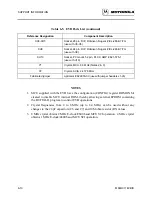
Page 94: ...OM 250 nS U4 I C MCM6164 8k RAM user supplied U5 I C MCM6164 8k RAM 250 nS U6 I C MC74HC138 decoder de multiplexer U7 I C MC74HC4066 MC14066B digital switch U8 I C MC1488P RS 232C driver U9 I C MC68B50P ACIA U10 I C MC68HC11A1FN MCU Note 1 U11 I C MC74HC74 D type flip flop U12 I C MC74HC14 inverter U13 I C MC74HC4040 binary ripple counter U14 I C MC1489P RS 232C receiver U15 Voltage detector 3 80 ...

Page 95: ... 4576 MHz Fabricated jumper Aptronics 929955 00 use with jumper headers J1 J6 NOTES 1 MCU supplied with the EVB have the configuration CONFIG register ROMON bit cleared to disable MCU internal ROM thereby allowing external EPROM containing the BUFFALO program to control EVB operations 2 Crystal frequencies from 4 to 8 MHz up to 8 4 MHz can be used without any changes to the 24 pF capacitors C6 and...

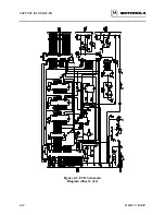
Page 96: ...SUPPORT INFORMATION M68HC11EVB D 6 11 11 6 4 DIAGRAMS Figure 6 2 is the EVB schematic diagram Figure 6 2 EVB Schematic Diagram Sheet 1 of 2 ...

Page 97: ...SUPPORT INFORMATION 6 12 M68HC11EVB D Figure 6 3 EVB Schematic Diagram Sheet 2 of 2 ...

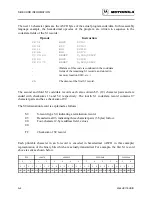
Page 98: ...s and the second the low order 4 bits of the byte The 5 fields which comprise an S record are shown below TYPE RECORD LENGTH ADDRESS CODE DATA CHECKSUM where the fields are composed as follows Field Printable Characters Contents Type 2 S record type S0 S1 etc Record length 2 The count of the character pairs in the record excluding the type and record length Address 4 6 or 8 The 2 3 or 4 byte addre...

Page 99: ... NOTE The EVB monitor supports only the S1 and S9 records All data before the first S1 record is ignored Thereafter all records must be S1 type until the S9 record terminates data transfer An S record format module may contain S records of the following types S0 The header record for each block of S records The code data field may contain any descriptive information identifying the following block...

Page 100: ...S9030000FC The above module consists of an S0 header record four S1 code data records and an S9 termination record The S0 header record is comprised of the following character pairs S0 S record type S0 indicating a header record 06 Hexadecimal 06 decimal 6 indicating six character pairs or ASCII bytes follow 00 00 Four character 2 byte address field zeroes 48 44 52 ASCII H D and R HDR 1B Checksum ...

Page 101: ...are ended with checksums 13 and 52 respectively The fourth S1 code data record contains 07 character pairs and has a checksum of 92 The S9 termination record is explained as follows S9 S record type S9 indicating a termination record 03 Hexadecimal 03 indicating three character pairs 3 bytes follow 00 00 Four character 2 byte address field zeroes FC Checksum of S9 record Each printable character i...

Page 102: ...N BUFFALO can be used with the MC68HC11 MCU in the single chip mode as shown in Figure C 1 The only terminal interface is through the SCI port Internally there are 54 bytes of RAM starting at 0000 and 512 bytes internal EEPROM which can be used for developing user programs ...

Page 103: ...APPLICATIONS B 2 M68HC11EVB D Figure B 1 Single Chip Mode Configuration ...

Reviews: