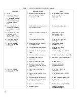
f.
Remove signal from X input terminals.
g.
Apply 0.7 Vdc (0.9 Vdc) to Y input terminals.
h.
Adjust R126 to position pen to full scale.
i.
In the event full scale cannot be reached by using
calibration controls, check electronic reference for output of 9.0
volts
±
5%.
5-96. PHASE SHIFT ADJUSTMENT
5-97. Assuming both X and Y axes have been adjusted by
means of the retrace curves described in paragraph 5-91, the
attenuator switches may be set to identical values in both X
and Y to produce a straight line of 45 degree angle. If the
retrace test made on X and Y demonstrates zero trace, the gap
which appears in the 45 degree retrace line will be due to a
phase difference or time lag between the two recording axes.
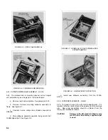
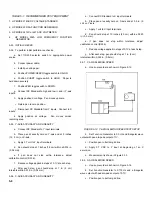
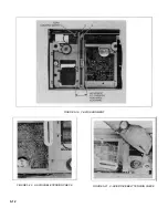
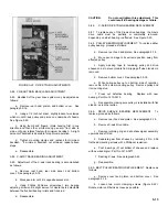
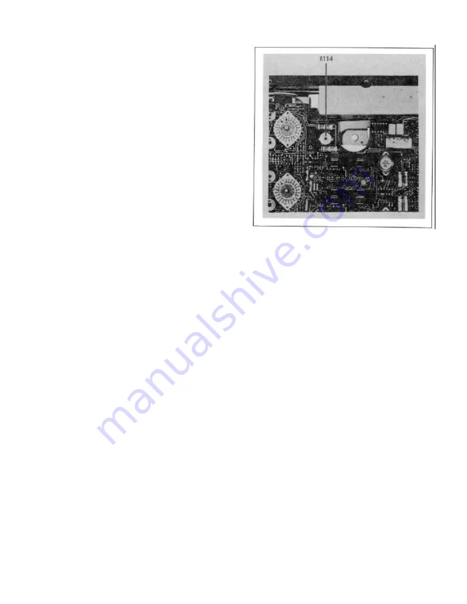
Phase adjust is accomplished by adjusting R114. Access to
R114 is obtained by removing bottom cover. See
paragraph 5-18 and Figure 5-24.
FIGURE 5-24. CIRCUIT BOARD ADJUSTMENT
5-15/5-16(blank)
Summary of Contents for HP-7035B
Page 1: ...TECHNICAL MANUAL HEWLETT PACKARD MODEL HP 7035B ...
Page 9: ...FIGURE 1 4 DIMENSION DRAWING FIGURE 1 5 ACCESSORIES 1 3 ...
Page 12: ...FIGURE 1 7 TYPICAL FREQUENCY RESPONSE INPUT FILTER FIGURE 1 8 TYPICAL DYNAMIC RESPONSE 1 6 ...
Page 14: ...FIGURE 2 1 WING BRACKET INSTALLATION FIGURE 2 2 STACKED CONFIGURATION 2 2 ...
Page 16: ...FIGURE 3 1 FRONT PANEL CONTROLS 7035B AND 7035B 001 MODELS 3 2 ...
Page 20: ...FIGURE 4 1 BLOCK DIAGRAM FIGURE 4 2 DETAILED BLOCK DIAGRAM 4 2 ...
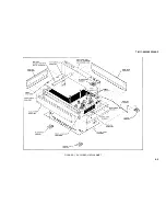
Page 48: ...TM 11 6625 2850 14 P FIGURE 6 1 EXPLODED VIEW CABINET 6 9 ...
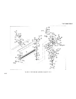
Page 49: ...TM 11 6625 2850 14 P FIGURE 6 2 EXPLODED VIEW CARRIAGE ARM SHEET 1 OF 2 6 10 ...
Page 58: ...FIGURE 7 1 COMPONENT IDENTIFICATION FRAME 7 8 ...
Page 59: ...TM 11 6625 2850 14 P Figure 7 2 Component Identification Circuit Board 7 9 ...
Page 60: ...TM 11 6625 2850 14 P Figure 7 3 Schematic Model 7035B D 07035 92550 7 10 ...
Page 62: ...TM 11 6625 2850 14 P FIGURE 8 1 COMPONENT IDENTIFICATION CIRCUIT BOARD 8 2 ...
Page 66: ...TM 11 6625 2850 14 P FIGURE 8 5 EXPLODED VIEW CARRIAGE ARM 8 6 ...

