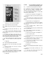
is used to pull sufficient quiescent current through Zener diode
CR-104, thereby holding its dynamic impedance at a
reasonable magnitude. Additional amplification is provided by
Q-106 which is capacitor coupled from Q-105 by C-121. The
voltage gain of the Voltage Amplifier is approximately 2000.
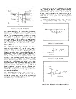
FIGURE 4-9. VOLTAGE AMPLIFIER
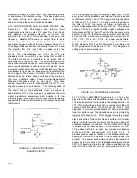
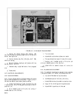
4-18. POWER AMPLIFIER/DEMODULATOR (See Figure 4-
10). This section can be roughly divided into two sections: the
first section provides the current gain required, and the last
provides both additional current gain and acts as a
demodulator. This stage consists of transistors Q-107, Q-108,
Q-109, and Q-110. Since this is essentially a Class B
operating stage, and the output section is a demodulator
applying half-wave ac to a permanent magnet dc servo motor,
operation of the demodulator section must first be understood
before discussing the entire output stage.
FIGURE 4-10. AMPLIFIER/DEMODULATOR
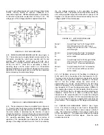
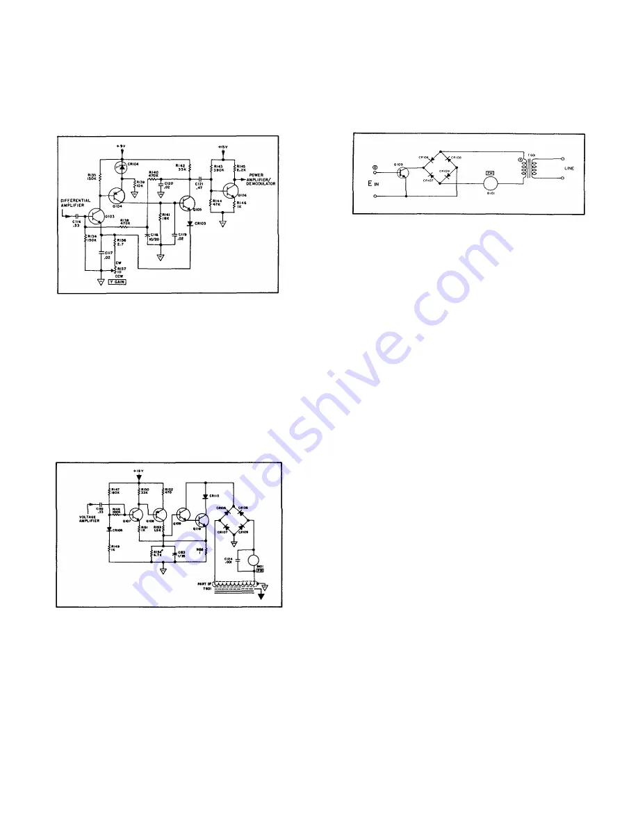
4-19. The demodulator is shown in simplified form in Figure 4-
11. Power to drive the dc servo motor is taken from a separate
shielded winding on power transformer T-601. The direction of
the motor rotation is determined by the direction of current
through the armature. Control of the motor current is provided
by the darlington pair comprised of transistors Q-109, and Q-
110, operating essentially Class B. The four modes of
operation of the demodulator are determined by the relative
phasing of the voltage at Points A and B. Point A is excited by
the line voltage appearing in the secondary of power
transformer T-601. The polarity of Point B is determined by the
error voltage amplifier output and will be either in phase or 180
degrees out of phase with the line as determined by the error
voltage applied to the photochopper.
FIGURE 4-11. MOTOR CONTROL AND
DEMODULATOR
Mode 1
Current flows from T-601, through B-101,
A-
CR-108, CR-110, Q-110, R-115, and
B+
through CR-107 back to T-601. The motor
will rotate right.
Mode 2
Current flowing from T-601 is blocked by
A-
Q-110. No current will flow, and motor
B-
will not rotate.
Mode 3
Current flows from T-601 through CR-106,
A+
CR-110, Q-110, R-155, CR-109, B-101
B+
back to T-601. The motor will rotate left.
Mode 4
Current flowing from T-601 is blocked by
A+
Q-110. No current will flow, and motor
B-
will not rotate.
4-20. AC feedback as well as dc feedback is obtained via
R-149 and R-155 to the emitter of the first transistor, Q-107.
The bias current at the input transistor is designed to pull the
output stage very slightly into Class A operation, to the extent
that at null, the voltage across the servo motor is
approximately 1/3 volt rms. Diode CR-105 in the bias string
helps to compensate for the temperature change of Vbe of the
input transistor Q-107 over the temperature range. Resistor R-
153, coupling the second and third transistor, limits the current
drain of Q-108 from the 15 volt supply when the output stage is
saturated. Diode CR-110 is used to minimize the power
dissipation in the output transistor Q-110 when the darlington
pair is saturated. Capacitor C-124 is connected directly across
the dc servo motor and serves to suppress RFI caused by the
motor brushes. The voltage gain of this stage is approximately
6.
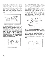
4-21. POWER AND REFERENCE SUPPLY (See Figure
4-12). The reference voltage for each axis is independents
derived from a Zener controlled dc power supply normally 9
volts. The temperature stability of this supply is better than
0.002% per degree C. This supply also furnished the voltage
for the servo amplifier's first three stages. Since the servo
amplifier input circuit
4-5
Summary of Contents for HP-7035B
Page 1: ...TECHNICAL MANUAL HEWLETT PACKARD MODEL HP 7035B ...
Page 9: ...FIGURE 1 4 DIMENSION DRAWING FIGURE 1 5 ACCESSORIES 1 3 ...
Page 12: ...FIGURE 1 7 TYPICAL FREQUENCY RESPONSE INPUT FILTER FIGURE 1 8 TYPICAL DYNAMIC RESPONSE 1 6 ...
Page 14: ...FIGURE 2 1 WING BRACKET INSTALLATION FIGURE 2 2 STACKED CONFIGURATION 2 2 ...
Page 16: ...FIGURE 3 1 FRONT PANEL CONTROLS 7035B AND 7035B 001 MODELS 3 2 ...
Page 20: ...FIGURE 4 1 BLOCK DIAGRAM FIGURE 4 2 DETAILED BLOCK DIAGRAM 4 2 ...
Page 48: ...TM 11 6625 2850 14 P FIGURE 6 1 EXPLODED VIEW CABINET 6 9 ...
Page 49: ...TM 11 6625 2850 14 P FIGURE 6 2 EXPLODED VIEW CARRIAGE ARM SHEET 1 OF 2 6 10 ...
Page 58: ...FIGURE 7 1 COMPONENT IDENTIFICATION FRAME 7 8 ...
Page 59: ...TM 11 6625 2850 14 P Figure 7 2 Component Identification Circuit Board 7 9 ...
Page 60: ...TM 11 6625 2850 14 P Figure 7 3 Schematic Model 7035B D 07035 92550 7 10 ...
Page 62: ...TM 11 6625 2850 14 P FIGURE 8 1 COMPONENT IDENTIFICATION CIRCUIT BOARD 8 2 ...
Page 66: ...TM 11 6625 2850 14 P FIGURE 8 5 EXPLODED VIEW CARRIAGE ARM 8 6 ...

