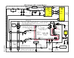


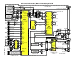

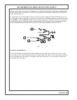


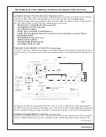

DP-3X HORIZONTAL DRIVE CIRCUIT EXPLANATION
PAGE 05-01
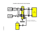
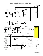
HORIZONTAL DRIVE CIRCUIT DIAGRAM DESCRIPTION:
(Use the Horizontal Drive Circuit Diagram for details)
CIRCUIT DESCRIPTION
When B+ arrives at the Rainforest IC
I501
pin (
45
), horizontal drive is output from pin (
37
). The drive signal is
routed through the connector
PPS3, PPD3
pin
6
to the Horizontal Driver Transistor
Q709
. This transistor
switches the ground return for pin (
8
) of the Driver transformer (
T702
).
SW+28
volts is routed through
R748
and
R730
. Then through
D715
and supplied to pin (
5
) as primary voltage. The switching of
Q709
allows EMF to
develop. As this signal collapses, it creates a pulse on the output pin of (
T702
) at pin (
4
) to the base of the De-
flection Horizontal output transistor
Q777
. This transistor provides primary switching pulses for the Deflection
Transformer
T701
.
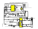
Q777 TRANSISTOR PRODUCES THE FOLLOWING OUTPUT PULSES;
1. The
Dynamic Focus OUT Circuit to QF01
: A Dynamic Focus waveform, (Horz. Parabola) is created.
This is a parabolic waveform that is superimposed upon the static focus voltage to compensate for beam
shape abnormalities which occur on the outside edges of the screen because the beam has to travel fur-
ther to those locations.
2. Horizontal Deflection Yokes drive signals.
The collector of
Q777
provides the drive signal for all
Horizontal Deflection Yokes.
T701 TRANSFORMER PRODUCES THE FOLLOWING OUTPUT PULSES;
•
Deflection H. Pulse from pin (7):
This pulse is used by;
HORIZONTAL BLANKING (H. BLK) GENERATED FROM PIN (7):
The Horizontal Pulse is also routed to the Horizontal Blanking generation transistor
Q706
. This transistor gener-
ates the 13V P/P called
H Blk
. This signal goes to the following circuits;
•
To the
PPD3, PPS3
connector pin
8
to pin (
39
) of
I501
as
FBP In.
Here this signal is used as a comparison
signal. It is compared to the reference signal coming in at pin (
50
) Horizontal Sync. If there are any differ-
ences between these two signals, the output Drive signal from pin (
37
) is corrected.
NOTE
: When a 1080i signal is input through component inputs, the Reference signal for Horizontal
Sync now becomes the H Sync before the Flex Converter. Output from sync selector
I502
, pin (
14)
.
(See the Main/Component Sync Circuit Diagram for details).
•
The H Blk signal is also routed to the Microprocessor which uses this signal for OSD positioning and for
Station Detection during Auto programming within the coincidence detector, also as a detection signal to
activate the AFC Loop.
•
The PinP unit uses this signal for switching purposes. Like the read/write clock, positioning, etc…
•
Through the
PDG
connector pin
14
to the Convergence circuit for correction waveform generation.
•
Through
CN01
to the Sweep Loss Circuit (
QN01
) to shut off the drive to the CRTs if Horizontal deflection
is lost.
H Blk for HORIZONTAL DRIVE FOR THE HIGH VOLTAGE CIRCUIT:
•
The Horizontal Blanking signal
H Blk
from
Q706
is also sent to the High Voltage Driver IC
IH01
pin (
3
).
This IC uses this signal as a Tickle Pulse signal to lock the high voltage H. Drive signal from
IH01
pin
1
.
The high voltage H. Drive signal is output pin
1
and routed to the driver transistors,
QH02
. Then to the High
Voltage Horizontal Output Transistor
QH01
. This transistor switches the primary of the Flyback transformer
TH01
. Deflection SW +115 is sent through pin (
9
) and output pin (
10
) to the collector of the Horizontal Out-
put Transistor
QH01
.
A sample of the High Voltage is output from the Flyback transformer
TH01
pin (
12
). This voltage is sent to pin
(
9
) of the High Voltage Driver IC
IH01
. This voltage is compared to the reference voltage available at pin (
12
).
(Continued on page 2)
Summary of Contents for 46W500
Page 2: ...DP 3X BLANK PAGE NOTES BLANK PAGE ...
Page 6: ...DP 3X BLANK PAGE NOTES BLANK PAGE ...
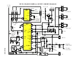
Page 7: ...DP 3X CHASSIS INFORMATION POWER SUPPLY INFORMATION SECTION 1 ...
Page 8: ...DP 3X BLANK PAGE NOTES BLANK PAGE ...
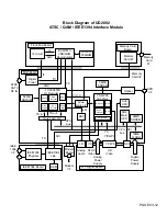
Page 23: ...DP 3X CHASSIS INFORMATION MICROPROCESSOR INFORMATION SECTION 2 ...
Page 24: ...DP 3X BLANK PAGE NOTES BLANK PAGE ...
Page 35: ...DP 3X CHASSIS INFORMATION VIDEO INFORMATION SECTION 3 ...
Page 36: ...DP 3X BLANK PAGE NOTES BLANK PAGE ...
Page 50: ...DP 3X BLANK PAGE NOTES BLANK PAGE ...
Page 51: ...DP 3X CHASSIS INFORMATION AUDIO INFORMATION SECTION 4 ...
Page 52: ...DP 3X BLANK PAGE NOTES BLANK PAGE ...
Page 57: ...DP 3X CHASSIS INFORMATION DEFLECTION INFORMATION SECTION 5 ...
Page 58: ...DP 3X BLANK PAGE NOTES BLANK PAGE ...
Page 69: ...DP 3X CHASSIS INFORMATION DIGITAL CONVERGENCE INFORMATION SECTION 6 ...
Page 70: ...DP 3X BLANK PAGE NOTES BLANK PAGE ...
Page 83: ...DP 3X CHASSIS INFORMATION ADJUSTMENT INFORMATION SECTION 7 ...
Page 84: ...DP 3X BLANK PAGE NOTES BLANK PAGE ...
Page 98: ...DP 3X BLANK PAGE NOTES BLANK PAGE ...
Page 99: ...DP 3X CHASSIS INFORMATION MISCELLANEOUS INFORMATION SECTION 8 ...
Page 100: ...DP 3X BLANK PAGE NOTES BLANK PAGE ...
Page 111: ...DP 3X CHASSIS INFORMATION DP 33W 46W500 DVD PLAYER TROUBLESHOOTING SECTION 9 ...
Page 112: ...DP 3X BLANK PAGE NOTES BLANK PAGE ...
Page 131: ...DP 3X CHASSIS INFORMATION THINGS YOU SHOULD KNOW SECTION 10 ...
Page 132: ...DP 3X BLANK PAGE NOTES BLANK PAGE ...
Page 134: ...DP 3X BLANK PAGE NOTES BLANK PAGE ...
Page 161: ...DP 3X BLANK PAGE NOTES BLANK PAGE ...
Page 162: ...DP 3X BLANK PAGE NOTES BLANK PAGE ...


