


XRM(2)-DAC-D4/1G User Guide
V2.2 - Mar 8, 2018
data output. This signal is normally controlled by the hardware pin (see register description below), but can be
controlled via the serial interface. SYNC is set low prior to clock adjustment ( and the FPGA-generated data
forced to output a zero level) to minimise transients on the DAC outputs. The configuration sequence for the
DAC does produce some transients however, a feature of the DAC itself rather than the board design.
2.10 Multiple DAC synchronisation
Multiple DAC synchronisation requires the use of the hardware SYNC pin; in addition the internal FIFOs of the
DACs to be synchronised must also be aligned with each other. This is achieved by ensuring that bits D5 and D4
of DAC register CONFIG5 are initially cleared and the SYNC pin is pulsed high then low. Following this, D5 is set
high and the drive to the DAC SYNC pin then set high. This synchronises the DAC outputs to within ± 1 DAC
clock cycle. See the relevant device data sheet for further information.
2.11 Clocking on Virtex4, Virtex5
DCLK, SYNC and data must be produced synchronously for the DAC. At maximum speed, the data rate required
is 500 MHz DDR. This is possible by using the 4:1 OSERDES components on Virtex4 and Virtex5 FPGAs.
On the XRC cards using Virtex4 and Virtex5 FPGAs, only regional clock inputs are available to XMC modules so
global clocks must be generated using these inputs since the data input pins typically span multiple regions.
There is an unknown (and unconstrainable) delay between the I/O pin and the BUFG input which must be taken
into account when doing this.
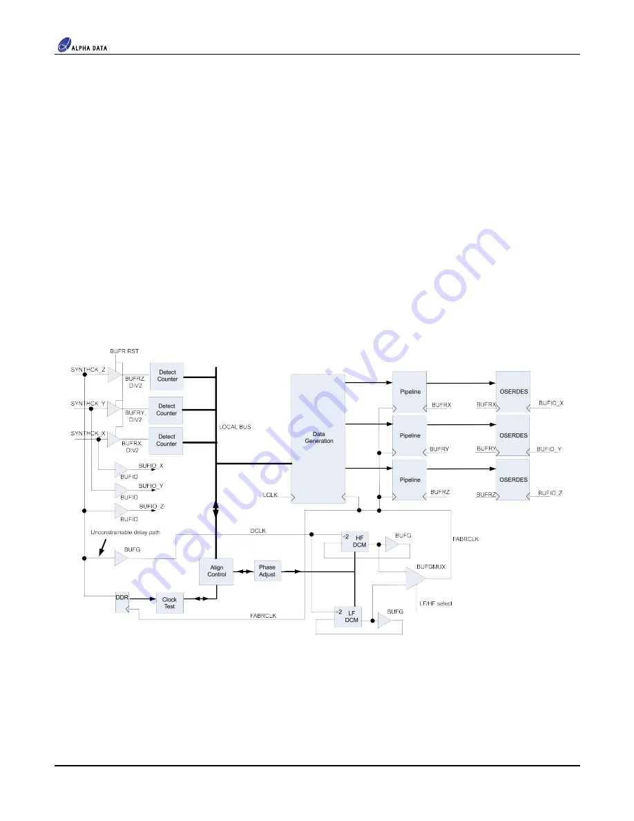
Figure 5 : Virtex 4 Virtex 5 Clocking Scheme
This delay is eliminated as shown in Figure Clocking Scheme. The clock input is fed to a pair of DCMs which
generates the clock required by the OSERDES circuitry. Two DCMs are required because of the input and
output clock restrictions of the DCM and the range of frequencies ( 125 MHz to 500MHz) which must be
produced. Each DCM uses a divide-by-2 pre-scaler to produce FABRCLK at the correct rate.
The output side of the OSERDES is clocked using a copy of the FPGA clock, appropriate to the clock region
occupied by the OSERDES. This is routed via a BUFIO to the OSERDES. The input side of the OSERDES is
Page 12
Hardware
xrm-dac-d4-1g-manual_v2_2.pdf


