


XRM(2)-DAC-D4/1G User Guide
V2.2 - Mar 8, 2018
can be used in this mode.Consult the factory for the availability of custom VCXO frequencies for applications
requiring other frequencies.
The external signal source can be used in place of the VCXO as the clock driving the distribution section for the
DAC so can be used as the DAC clock directly or integer divisions of this source can be used.The maximum
input frequency is 1.2 GHz
See the AD9510 data sheet for further information.
2.7 DAC Selftest
The DAC has a number of self-test capabilities built in which are implemented in the example code.
2.7.1 Pattern testing
This consists of writing values of 0xAAAA and 0X5555 in succession. Error flags can be interrogated via the
serial interface to determine the success or otherwise of the data transfers and thereby test the FPGA-DAC
interface.
2.7.2 Fifo Test
The DAC provides the facility to check for FIFO overruns, which normally should not occur. For applications
where low-level control of register bits has been implemented ( e.g. FIFO_offset position), this provides
confirmation of correct fifo operation.
2.7.3 Selftest
This runs an internal self-test algorithm which requires 400,000 DACCLK cycles, so completes in < 1ms for a
1GHz clock frequency. Pass/fail flags can be interrogated via the serial interface
2.8 DAC DLL Control
The DAC uses a DLL to align its input registers with DCLK and hence with the data. Any change in the DAC
clock frequency (thus DCLK and FABRCLK) requires the DLL control bits in DAC register CONFIG10 to be set
appropriately and the DLL re-aligned. This in turn requires the application of a hardware reset as part of the
initialisation sequence so any existing settings will be lost. These settings must be explicitly re-written as part of
the sequence.
The DLL control register (address 0xA) in the DAC has several different bit fields listed in the data sheet.
Effectively these can be treated as a single bit field since the values to be used for each frequency are fixed
( see "Electrical Characteristics" in the relevant device data sheet). Note that the frequency break points for the
DAC5682Z changed from (200,300) and (300,500) to (200,325) and (325,500) in the March 09 data sheet.
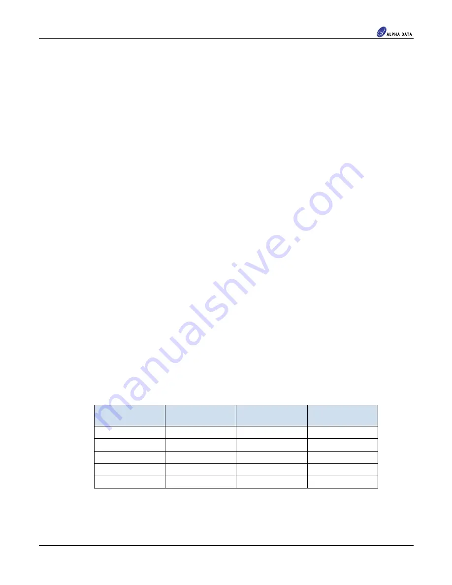
DAC5681 DCLK
(MHz)
DAC5681Z DCLK
(MHz)
DAC5682Z DCLK
(MHz)
Setting
125-150
125-150
125-150
0xCD
150-175
150-175
150-175
0xCE
175-200
175-200
175-200
0xCF
200-325
200-325
200-325
0xC8
325-500
325-500
325-500
0xC0
2.9 DAC Sync
The DAC configuration sequence requires a rising edge to be generated on the internal SYNC signal to instigate
Page 11
Hardware
xrm-dac-d4-1g-manual_v2_2.pdf


