


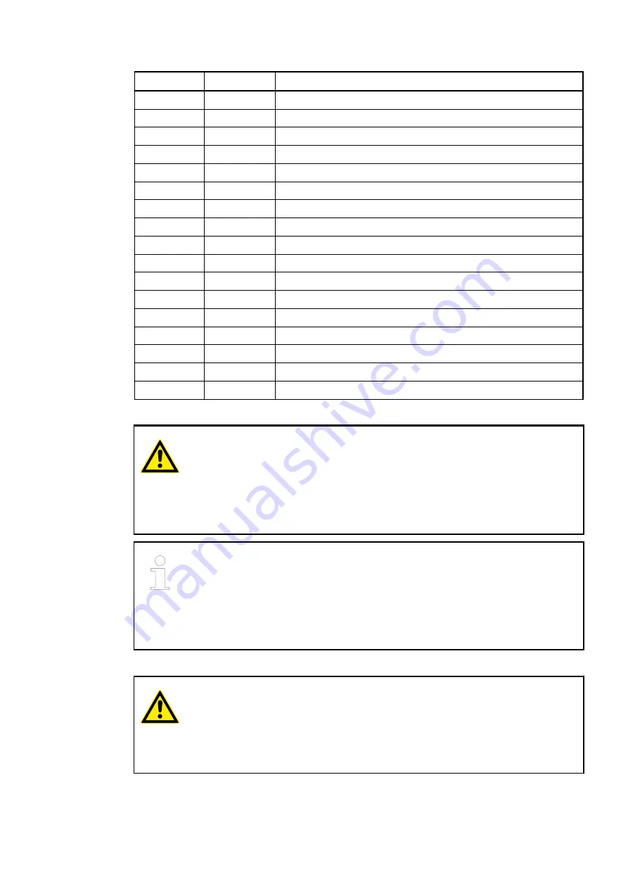
Terminal
Signal
Description
1.9
M
Process voltage M (0 VDC)
2.0...2.7
AI0-...AI7-
Negative input signal AI0...AI7 for analog channel 0...7
2.8/2.9
DI0/DI1
Input signal I0/I1 (standard digital input)
3.0...3.7
AI0+...AI7+
Positive input signal AI0...AI7 for analog channel 0...7
3.8/3.9
DC2/DC3
Signal of configurable digital input/output C2/C3
4.0...4.7
SH
Shield connection
4.8
L+
Process voltage L+ (24 VDC)
4.9
M
Process voltage M (0 VDC)
5.0...5.7
AI8-...AI15-
Negative input signal AI0AI7 for analog channel 8...15
5.8
L+
Process voltage L+ (24 VDC)
5.9
M
Process voltage M (0 VDC)
6.0...6.7
AI8+...AI15+
Positive input signal AI0...AI7 for analog channel 8...15
6.8
L+
Process voltage L+ (24 VDC)
6.9
M
Process voltage M (0 VDC)
7.0...7.7
SH
Shield connection
7.8
L+
Process voltage L+ (24 VDC)
7.9
M
Process voltage M (0 VDC)
CAUTION!
Risk of damaging the PLC modules!
The PLC modules must not be removed while the plant is connected to a power
supply.
Make sure that all voltage sources (supply and process voltage) are switched
off before you remove or replace a module.
Analog signals must be transmitted through shielded cables. The analog cable
shield must only be connected to the side of the module (SH terminals) to avoid
relaxation currents influencing the measuring results and for optimal robustness
against external noise. The shield connection must be as short as possible (< 3
cm). The analog shield is capacitive and internally coupled with the functional
earth (FE). To avoid unacceptable potential differences between different parts
of the installation, low-resistance equipotential bonding conductors must be laid.
CAUTION!
Risk of damaging the processor module and terminal base!
Voltages surpassing the permitted range might damage the processor module
and terminal base.
Never connect supply and process voltages
>
30 VDC to the terminal base.
Device Specifications
Terminal Bases (AC500 Standard) > TF501-CMS and TF521-CMS - Function Module Terminal Bases
2019/04/17
3ADR010121, 13, en_US
16