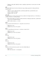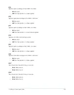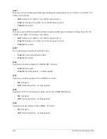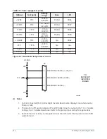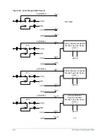
The RS-232 voltages are industry st5 to +25VDC and -5VDC to -25VDC logic levels. The
RS-485 voltages are industry standard 0VDC and +1.5VDC to +5VDC logic levels.
A diagnostic test can be performed on each serial port to confirm proper operation. Refer to
Diagnostics Section of
Form 160.54-M1
for details.
The LED’s and their functions are as follows:
•
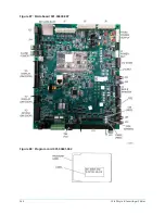
CR41 RX1 – COM1 serial port receive data.
•
CR42 TX1 – COM1 serial port transmit data.
•
CR40 RX2 – COM2 serial port receive data.
•
CR37 TX2 – COM2 serial port transmit data.
•
CR38 RX3 – COM3 serial port receive data.
•
CR35 TX3 – COM3 serial port transmit data.
•
CR39 RX4 – COM4 serial port receive data.
•
CR36 TX4 – COM4 serial port transmit data.
•
CR44 RX5B – COM5B serial port receive data.
•
CR43 TX5B – COM5B serial port transmit data.
•
CR48 RX6 – COM6 serial port receive data.
•
CR46 TX3 – COM6 serial port transmit data.
Display interface
The graphic screens displayed on the Liquid Crystal Display are created from the program
downloaded from the Program card and stored in the Flash Memory Chip. The data to form these
screens is output from J5. This data is in the form of red, green and blue drive signals applied
to each of the 303,200 display pixels arranged in a matrix of 640 columns x 480 rows. Each pixel
consists of 3 windows; red, green and blue, through which a variable amount of light from the
Display Backlight, is permitted to pass to the front of the display. The drive signals determine the
amount of light permitted to pass through each window. The overall pixel color is a result of the
gradient of red, green and blue light allowed to pass. The drive signal for each pixel is an 18 bit
binary word; 6 for each of the 3 colors. The greater the binary value, the more light is permitted to
pass. The pixels are driven sequentially from left to right, beginning with the top row. To coordinate
the drive signals and assure the pixels in each row are driven from left to right and the columns are
driven from top to bottom, the drive signals are accompanied by a clock and horizontal and vertical
sync signals.
During the boot-up, the program in the FeRAM reads wire jumpers PID0 through PID3 on the
Display Interface Board to determine the manufacturer of the display. Each display manufacturer
requires a slightly different control. The program in the BIOS EPROM configures the microboard for
correct operation for the actual display installed.
Different display manufacturers require different supply and control voltages for their displays
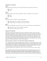
and backlights. Program Jumpers JP2 through JP5 and JP7 and JP8 must be configured to provide
the required supply and control voltages to the display and backlight control. A label attached to
the display mounting plate lists the required program jumper configuration for that display. The
position of program jumper JP2 determines whether the supply voltage is +5VDC or +3.3VDC.
The microboard controls the Display Backlight via J6. The Display Backlight is the light source
for the display. The Backlight Inverter Board (FL Backlight Displays) provides a high voltage AC
power source for the lamp. It converts low voltage DC via J6-1 (+12VDC or +5VDC, depending
on position of Program Jumper JP5) to high voltage AC (500 to 1500VAC). This high voltage AC is
applied to the lamp to cause it to illuminate. The Backlight is turned ON and OFF with the “Backlight
Enable” signal (J6-5). The position of Program Jumper JP4 determines whether this is a +12VDC or
251
YK-EP Style B Centrifugal Chiller
Содержание YK-EP
Страница 2: ...2 YK EP Style B Centrifugal Chiller...
Страница 6: ...6 YK EP Style B Centrifugal Chiller...
Страница 227: ...Figure 72 Sample printout of Status 227 YK EP Style B Centrifugal Chiller...
Страница 228: ...Figure 73 Sample printout of Status cont YK EP Style B Centrifugal Chiller 228...
Страница 229: ...Figure 74 Sample printout of Setpoints 229 YK EP Style B Centrifugal Chiller...
Страница 230: ...Figure 75 Sample printout of Setpoints cont YK EP Style B Centrifugal Chiller 230...
Страница 231: ...Figure 76 Sample printout of Schedule 231 YK EP Style B Centrifugal Chiller...
Страница 232: ...Figure 77 Sample printout of a Sales order YK EP Style B Centrifugal Chiller 232...
Страница 233: ...Figure 78 Sample printout of a Sales order cont 233 YK EP Style B Centrifugal Chiller...
Страница 234: ...Figure 79 Sample printout of History YK EP Style B Centrifugal Chiller 234...
Страница 235: ...Figure 80 Sample printout of History cont 235 YK EP Style B Centrifugal Chiller...
Страница 236: ...Figure 81 Sample printout of a security log report YK EP Style B Centrifugal Chiller 236...
Страница 260: ...Figure 87 Microboard 031 03630 007 Figure 88 Program card 031 03601 002 YK EP Style B Centrifugal Chiller 260...


