


Chapter 2
Connecting Signals
NI PXI-4220 User Manual
2-2
ni.com
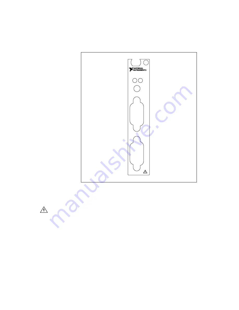
Figure 2-1.
NI PXI-4220 Front Label
Construct a signal lead with an SMB connection to connect a timing or
triggering signal to the PFI0/CAL SMB connector.
Caution
The PFI0/CAL SMB connector is for low-voltage timing and calibration signals
only
. Voltages greater than ±10 V can damage the device.
Figure 2-2 shows the pin signal assignments for each of the NI PXI-4220
D-SUB connectors. Refer to Figure 2-2 when constructing D-SUB
connection leads to ensure the signal wires are routed correctly. In the
electrical connection diagram, each signal connection node is labeled with
a pin number to indicate which pin carries the signal.
2 Channel Bridge Input
ACCESS
ACTIVE
AI 0
AI 1
PFI 0/
CAL
NI PXI-4220
Artisan Technology Group - Quality Instrumentation ... Guaranteed | (888) 88-SOURCE | www.artisantg.com


