Functional Description
http://www.motorola.com/computer/literature
2-43
2
When not being loaded, the timer will continuously decrement itself until
either reloaded by software or a count of zero is reached. If a timer reaches
a count of zero, an output signal will be asserted and the count will remain
at zero until reloaded by software or PHB reset is asserted. External logic
can use the output signals of the timers to generate interrupts, machine
checks, etc.
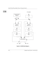
Each timer is composed of a prescaler and a counter. The prescaler
determines the resolution of the timer, and is programmable to any binary
value between 1 microseconds and 32,768 microsecons. The counter
counts in the units provided by the prescaler. For example, the watchdog
timer would reach a count of zero within 24 microseconds if the prescaler
was programmed to 2 microseconds and the counter was programmed to
12.
The watchdog timers are controlled by registers mapped within the PPC
control register space. Each timer has a WDTxCNTL register and a
WDTxSTAT register. The WDTxCNTL register can be used to start or
stop the timer, write a new reload value into the timer, or cause the timer
to initialize itself to a previously written reload value. The WDTxSTAT
register is used to read the instantaneous count value of the watchdog
timer.
Programming of the Watchdog Timers is performed through the
WDTxCNTL register and is a two step process.
❏
Step 1 is to ‘arm’ the WDTxCNTL register by writing
PATTERN_1 into the KEY field. Only the KEY byte lane may be
selected during this process. The WDTxCNTL register will not arm
itself if any of the other byte lanes are selected or the KEY field is
written with any other value than PATTERN_1. The operation of
the timer itself remains unaffected by this write.
❏
Step 2 is to write the new programming information to the
WDTxCNTL register. The KEY field byte lane must be selected
and must be written with PATTERN_2 for the write to take affect.
The effects on the WDTxCNTL register depend on the byte lanes
that are written to during step 2 and are shown in Table 2-14.
Содержание MVME5100 Series
Страница 1: ...MVME5100 Single Board Computer Programmer s Reference Guide V5100A PG2 September 2001 Edition ...
Страница 16: ...xvi ...
Страница 20: ...xx ...
Страница 28: ...xxviii ...
Страница 62: ...1 34 Computer Group Literature Center Web Site Product Data and Memory Maps 1 ...
Страница 278: ...3 88 Computer Group Literature Center Web Site System Memory Controller SMC 3 ...
Страница 288: ...4 10 Computer Group Literature Center Web Site Hawk Programming Details 4 ...
Страница 320: ...Index IN 12 Computer Group Literature Center Web Site I N D E X ...


