REL0.1
Page 16 of 95
Kintex Ult FPGA SOM Hardware User Guide
iWave Systems Technologies Pvt. Ltd.
2.3.1.3
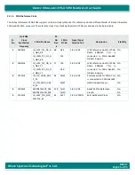
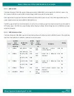
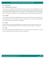
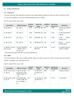
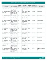
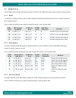
FPGA Reference Clock
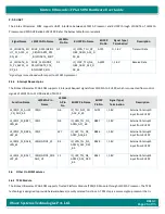
The Kintex Ult FPGA SOM supports on board clock synthesizer for reference clock to different blocks of Kintex Ult
FPGA and LS1021A processor. The reference clock from Clock Synthesizer to FPGA is mentioned in the below table.
Sl.
No
On-SOM
Clock
Synthesizer
Frequency
FPGA Pin Name
FP
GA
Ban
k
FPGA
Pin No
Signal Type/
Termination
Description
Stability
1
300MHz
IO_L13P_T2L_N0_G
C_QBC_68
68
G14
1.8V, LVDS
LVDS reference clock for FPGA
DDR4
SDRAM1.
This
is
connected to FPGA Bank68
Global clock pins.
NA
IO_L13N_T2L_N1_G
C_QBC_68
F14
2
300MHz
IO_L13P_T2L_N0_G
C_QBC_71
71
J26
1.8V, LVDS
LVDS reference clock for FPGA
DDR4
SDRAM2.
This
is
connected to FPGA Bank71
Global clock pins.
NA
IO_L13N_T2L_N1_G
C_QBC_71
H26
NA
3
125MHz
IO_L7P_HDGC_AD5
P_92
92
AN22
1.8V, LVDS
Reference clock for FPGA. This
is connected to FPGA Bank92
HDGC Global clock pin.
NA
IO_L7N_HDGC_AD5
N_92
AN21
NA
4
100MHz
MGTREFCLK0P_228
228 AH11
1.8V, LVDS
Bank228 PCIe Reference
Clock0.
NA
MGTREFCLK0N_228
AH10
NA
5
125MHz
IO_L24P_T3U_N10_
EMCCLK_65
65
AL27
1.8V, LVCMOS
External Master Clock
NA


