REL0.1
Page 15 of 95
Kintex Ult FPGA SOM Hardware User Guide
iWave Systems Technologies Pvt. Ltd.
2.3.1.1
FPGA Power
The Kintex Ult FPGA SOM uses discrete power regulators along with DA9062 PMIC from Dialog Semiconductor for FPGA
power management. In SOM, FPGA power domain supply voltage (VCC_INT, VCCINT_IO, VCCBRAM) is fixed to 0.85V or 0.9V based
on the speed grade of the FPGA.
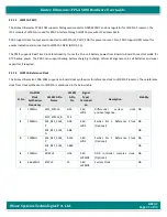
The Kintex Ult FPGA SOM supports Dialog semiconductor DA9062 PMIC for other powers to FPGA. The I2C2 module of
LS1021A is used for FPGA PMIC interface with I2C address 0x48. The I/O voltage of HD Bank (PL Bank 92) and HP Banks (Bank 65,
66 & 67) which are connected to Board-to-Board Connectors are generated from PMIC LDO1, LDO2, LDO3 and LDO4 respectively.
PMIC’s LDO1 is connected to I/O voltage of H
D Bank92 and by default set to 1.2V, LDO2 is connected to I/O voltage of HP Bank65
and by default set to 1.8V, LDO3 is connected to HP Bank66 and by default set to 1.0V, LDO4 is connected to I/O voltage of HP
Bank67 and by default set to 1.0V. IO voltage is configurable through software after LS1021A boot-up.
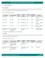
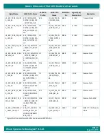
PMIC supports reset output and connected to Kintex Ult FPGA AL28 pin (IO_L24N_T3U_N11_DOUT_CSO_B_65) for power
on reset. Also, PMIC supports IRQ output for events indication and connected to FPGA BC28 pin (IO_T1U_N12_SMBALERT_65).
Important Note: Every Power Off and On, The DA9062 PMIC work as initial OTP Setting
2.3.1.2
FPGA Reset
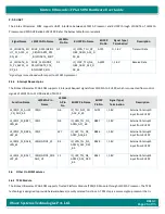
The Kintex Ult FPGA
SOM uses PMIC’s Reset output (nRESET) for FPGA Power On Reset and connected to AL28 pin
(IO_L24N_T3U_N11_DOUT_CSO_B_65) of FPGA.


