background image


REL0.1 

Page 54 of 95 

Kintex Ult FPGA SOM Hardware User Guide


iWave Systems Technologies Pvt. Ltd. 

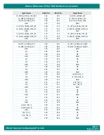
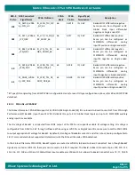
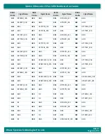
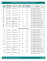
B2B-2 

Pin No 

B2B Connector2 

Signal Name 

FPGA Pin Name 

FPGA 

Bank 

FPGA 

Pin No 

Signal Type/ 

Termination* 

Description 

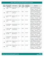
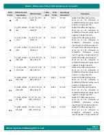
152 

PL_BE17_LVDS66
_L1P_DBC 

IO_L1P_T0L_N0_D
BC_66 

66 

BE17 

IO, 1.8V 

Bank66 IO1 differential positive. 
Same pin can be configured as Single 
ended I/O. 

154 

PL_BF17_LVDS66
_L1N_DBC 

IO_L1N_T0L_N1_
DBC_66 

66 

BF17 

IO, 1.8V 

Bank66 IO1 differential negative. 
Same pin can be configured as Single 
ended I/O. 

156 

PL_AR17_LVDS66
_L16P_QBC 

IO_L16P_T2U_N6
_QBC_AD3P_66 

66 

AR17 

IO, 1.8V 

Bank66 IO16 differential positive. 
Same  pin  can  be  configured  as 
PLSYSMON 

differential 

analog 

input3 positive or Single ended I/O. 

158 

PL_AT17_LVDS66
_L16N_QBC 

IO_L16N_T2U_N7
_QBC_AD3N_66 

66 

AT17 

IO, 1.8V 

Bank66 IO16 differential negative. 
Same  pin  can  be  configured  as 
PLSYSMON 

differential 

analog 

input3 negative or Single ended I/O. 

160 

PL_BF18_LVDS66
_L2N 

IO_L2N_T0L_N3_6

66 

BF18 

IO, 1.8V 

Bank66 IO2 differential negative. 
Same pin can be configured as Single 
ended I/O. 

162 

PL_BF19_LVDS66
_L2P 

IO_L2P_T0L_N2_6

66 

BF19 

IO, 1.8V 

Bank66 IO2 differential positive. 
Same pin can be configured as Single 
ended I/O. 

164 

PL_AT18_LVDS66
_L15P 

IO_L15P_T2L_N4_
AD11P_66 

66 

AT18 

IO, 1.8V 

Bank66 IO15 differential positive. 
Same  pin  can  be  configured  as 
PLSYSMON 

differential 

analog 

input11 positive or Single ended I/O. 

166 

PL_AU17_LVDS6
6_L15N 

IO_L15N_T2L_N5_
AD11N_66 

66 

AU17 

IO, 1.8V 

Bank66 IO15 differential negative. 
Same  pin  can  be  configured  as 
PLSYSMON 

differential 

analog 

input11  negative  or  Single  ended 
I/O. 

170 

PL_AV19_LVDS6
6_L12P_GC 

IO_L12P_T1U_N1
0_GC_66 

66 

AV19 

IO, 1.8V 

Bank66 IO12 differential positive 
Same  pin  can  be  configured  as  GC 
Global  Clock  Input  differential 
positive or Single ended I/O. 

172 

PL_AW19_LVDS6
6_L12N_GC 

IO_L12N_T1U_N1
1_GC_66 

66 

AW19 

IO, 1.8V 

Bank66 IO12 differential negative 
Same  pin  can  be  configured  as  GC 
Global  Clock  Input  differential 
negative or Single ended I/O. 

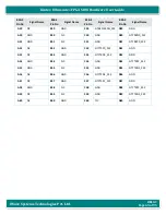
176 

PL_AV18_LVDS6
6_L11P_GC 

IO_L11P_T1U_N8
_GC_66 

66 

AV18 

IO, 1.8V 

Bank66 IO11 differential positive 
Same  pin  can  be  configured  as  GC 
Global  Clock  Input  differential 
positive or Single ended I/O. 
Содержание iW-RainboW-G47M

Страница 1: ...REL0 1 Page 1 of 95 Kintex Ultrascale FPGA SOM Hardware User Guide iWave Systems Technologies Pvt Ltd iW RainboW G47M Kintex Ultrascale FPGA SOM Hardware User Guide...

Страница 2: ...document contains proprietary material for the sole use of the intended recipient s Do not read this document if you are not the intended recipient Any review use distribution or disclosure by others...

Страница 3: ...n errata and associated issues Trademarks All registered trademarks product names mentioned in this publication are the property of their respective owners and used for identification purposes only Ce...

Страница 4: ...ion Status 17 2 3 1 5 FPGA Mode Configuration 18 2 3 1 6 FPGA System Monitor ADC 18 2 3 2 FPGA Memory 19 2 3 2 1 DDR4 SDRAM1 with ECC 19 2 3 2 2 DDR4 SDRAM2 with ECC 19 2 4 Layerscape Processor 20 2 4...

Страница 5: ...Interfaces 50 2 8 2 1 FPGA IOs HP BANK66 65 50 2 8 2 2 FPGA IOs HP BANK67 55 2 8 3 Power Reset Input 61 2 9 Board to Board Connector3 62 2 9 1 FPGA Interfaces 66 2 9 1 1 GTY High Speed Transceivers 66...

Страница 6: ...REL0 1 Page 6 of 95 Kintex Ultrascale FPGA SOM Hardware User Guide iWave Systems Technologies Pvt Ltd 5 APPENDIX 94 5 1 Kintex Ultrascale FPGA SOM Development Platform 94...

Страница 7: ...nical dimension of Kintex Ultrascale FPGA SOM Top View 90 Figure 12 Mechanical dimension of Kintex Ultrascale FPGA SOM Bottom View 91 Figure 13 Mechanical dimension of Kintex Ultrascale FPGA SOM Side...

Страница 8: ...high speed ruggedized terminal strip connectors and Two High Speed High Density connectors provide the carrier board interface to carry all the I O signals to and from the Kintex Ultrascale FPGA SOM...

Страница 9: ...erminology is used Table 2 Terminology Terminology Description I Input Signal O Output Signal IO Bidirectional Input output Signal CMOS Complementary Metal Oxide Semiconductor Signal LVDS Low Voltage...

Страница 10: ...High Speed Connector3 240Pin Board to Board High Speed Connector4 80Pin FPGA IOs DDR4 64bit 8bit ECC Bank 69 70 71 DDR4 4GB Bank 72 73 74 DDR4 4GB Bank 228 2 0 229 230 231 232 GTY Transceiver Bank 225...

Страница 11: ...ackplane capable transceivers PMIC Dialog s DA9062 PMIC RTC is optional Memory 4GB DDR4 SDRAM1 64bit with 8 bit ECC Expandable 4GB DDR4 SDRAM2 64bit with 8 bit ECC Expandable 128MB QSPI Flash CPU QorI...

Страница 12: ...B 3 0 x 1 1 SerDes lane for high speed peripheral interface with reference clock 6 GPIOs From LS1021A From KU19P GTY High Speed Transceivers up to 32 75Gbps x 8 FPGA IOs HD Bank 92 Up to 11 LVDS IOs 2...

Страница 13: ...ifferential Single Ended FPGA IOs HP Bank 67 Up to 22 LVDS IOs 44 Single ended SE IOs o Up to 4 GC Global Clock Input pins LVDS SE o Up to 15 ADC Input pins Differential Single Ended Board to Board Co...

Страница 14: ...the latest Kintex Ultrascale FPGA Datasheet Technical ReferenceManual for more details which may be revised from time to time Figure 2 Kintex Ultrascale FPGA Devices Comparison The Kintex Ultrascale...

Страница 15: ...nerated from PMIC LDO1 LDO2 LDO3 and LDO4 respectively PMIC s LDO1 is connected to I O voltage of HD Bank92 and by default set to 1 2V LDO2 is connected to I O voltage of HP Bank65 and by default set...

Страница 16: ...00MHz IO_L13P_T2L_N0_G C_QBC_68 68 G14 1 8V LVDS LVDS reference clock for FPGA DDR4 SDRAM1 This is connected to FPGA Bank68 Global clock pins NA IO_L13N_T2L_N1_G C_QBC_68 F14 2 300MHz IO_L13P_T2L_N0_G...

Страница 17: ...he Kintex Ultrascale FPGA SOM supports two LEDs for the Program Done indication and Power LED indication LED D2 is for PROG_DONE and it is asserted for DONE indicates successful completion of configur...

Страница 18: ...Ultrascale FPGA contain one System Monitor block SYSMONE4 It is used to enhance the overall safety security and reliability of the system by monitoring the physical environment via on chip power supp...

Страница 19: ...pling capacitors Note Kintex Ultrascale FPGA SOM with 2 3 speed grade FPGA can support up to 2666Mbps data rate for FPGA DDR4 2 3 2 2 DDR4 SDRAM2 with ECC The Kintex Ultrascale FPGA SOM supports 64bit...

Страница 20: ...running up to 1 2 GHz and providing pre silicon CoreMark performance of over 5 000 the LS102xA family delivers greater performance than any previous sub 4W communication processor The Block Diagram of...

Страница 21: ...p battery charging to charge Lithium Manganese coin cell batteries and super capacitors if required 2 4 1 3 LS1021A Reference Clock The Kintex Ultrascale FPGA SOM supports on board clock synthesizer f...

Страница 22: ...ensity 16bit DDR4 device 2 4 2 2 NOR Flash The Kintex Ultrascale FPGA SOM supports 250MB NOR Flash memory as boot device of LS1021A Processor The NOR Flash is used for programming RCW and U boot for L...

Страница 23: ...e KU19P Pin No Signal Type Termination Description LS_SD1_RX0_P SD1_RX0_P AC10 MGTYTXP3_228 AF7 I DIFF SerDes Receive Data0 positive LS_SD1_RX0_N SD1_RX0_N AB10 MGTYTXN3_228 AF6 I DIFF SerDes Receive...

Страница 24: ...D26 O 1 8V Transmit Enable LS_EC3_RXCLK_PL_BE 28_L3N_65 EC3_RX_CLK GPIO4 _07 TSEC_1588_CL K_IN FTM3_QD_PH A V2 IO_L3N_T0L_N5 _AD15N_A27_6 5 BE28 I 1 8V Receive Clock LS_EC3_RXD0_PL_BD 28_L3P_65 EC3_RX...

Страница 25: ...LS1021A to KU19P which is connected from control signals of LS1021A to PL HP Bank 65 of KU19P Function Name LS1021A Pin Name LS1021 A Pin No KU19P Pin Name KU19P Pin No Signal Type Termination Descrip...

Страница 26: ...d to the SPI2 lane of LS1021A and operates at 1 8V Voltage level 2 6 2 Temperature Sensor The Kintex Ultrascale FPGA SOM supports Temperature sensor through both LS1021A Processor and KU19P SoC In the...

Страница 27: ...design to provide the maximum interfaces of Kintex Ultrascale FPGA to the carrier board by adding these two Board to Board Connectors The Kintex Ultrascale FPGA SOM Board to Board Connector1 pinout i...

Страница 28: ...GND PL_AV24_LVDS92_L2P 27 28 LS_GPIO3_18 EC2_TXD0 PL_AW24_LVDS92_L2N 29 30 LS_GPIO3_17 EC2_TXD1 PL_AL24_LVDS92_L10P 31 32 LS_GPIO3_24 EC2_RXD1 PL_AM24_LVDS92_L10N 33 34 LS_GPIO4_09 TDMA_RXD GND 35 36...

Страница 29: ...C GTYRXP1_226 111 112 NC GND 113 114 GND GTYRXN0_226 115 116 PL_AV28_LVDS65_L14N_A05_D21_GC GTYRXP0_226 117 118 PL_AV27_LVDS65_L14P_A04_D20_GC GND 119 120 GND GND 121 122 GND GTYTXP2_226 123 124 PL_AV...

Страница 30: ...EFCLK0N_124 GND 187 188 GND GTYTXP1_124 189 190 PL_AM14_LVDS67_L24N GTYTXN1_124 191 192 PL_AL14_LVDS67_L24P GND 193 194 PL_AT13_T3U_N12_67 GTYRXN1_124 195 196 PL_AT14_T2U_N12_67 GTYRXP1_124 197 198 PL...

Страница 31: ...Data Positive 2 7 1 2 SerDes Interface The Kintex Ultrascale FPGA SOM supports 1 highspeed SerDes lane and its reference clock through LS1021A Layerscape Processor in board to board connector1 For mor...

Страница 32: ...D00 H3 I 3V3 General Purpose I O from LS1021A Processor 38 LS_GPIO3_19 EC2_T XEN EC2_TX_EN GP IO3_19 USB2_ STP FTM2_FA ULT T5 O 3V3 General Purpose I O from LS1021A Processor 2 7 2 FPGA Interfaces The...

Страница 33: ...Pins 3 GTYTXP0_225 MGTYTXP0_225 225 BF5 O DIFF GTY Bank225 channel0 High speed differential transmitter positive 5 GTYTXN0_225 MGTYTXN0_225 225 BF4 O DIFF GTY Bank225 channel0 High speed differential...

Страница 34: ...MGTYTXN0_226 226 AU8 O DIFF GTY Bank226 channel0 High speed differential transmitter negative 103 GTYTXP1_226 MGTYTXP1_226 226 AT7 O DIFF GTY Bank226 channel1 High speed differential transmitter posi...

Страница 35: ...to 22 PLSYSMON auxiliary analog inputs are available The IO voltage of Bank92 is connected from LDO1 output of the PMIC and supports variable IO voltage setting IO voltage is configurable from 1 2V to...

Страница 36: ...positive Same pincan be configured as HDGC Global Clock Input differential positive or PLSYSMON differential analog input6 negative or Single ended I O 89 PL_AU24_LVDS9 2_L6N_HDGC IO_L6N_HDGC _AD6N_92...

Страница 37: ...as HDGC Global Clock Input differential negative or PLSYSMON differential analog input4 negative or Single ended I O 24 PL_AN23_LVDS9 2_L8P_HDGC IO_L8P_HDGC_ AD4P_92 92 AN23 IO 3 3V Bank92 IO8 differ...

Страница 38: ...x KU19P FPGA datasheet 2 7 2 3 FPGA IOs HP BANK65 67 The Kintex Ultrascale FPGA SOM supports 4 DIFF IOs 9 Single Ended SE IOs on Board to Board Connector1 from FPGA High Performance HP Bank65 and 1 DI...

Страница 39: ...k65 IO14 differential negative Same pin can be configured as GC Global Clock Input differential positive or Single ended I O 118 PL_AV27_LVDS6 5_L14P_A04_D2 0_GC IO_L14P_T2L_N 2_GC_A04_D20 _65 65 AV27...

Страница 40: ...Control Input The Kintex Ultrascale FPGA SOM works with 5V power input VCC from Board to Board Connector2 and generates all other required powers internally On SOM itself SOM power can be enabled dis...

Страница 41: ...rovided in the below table and the interfaces which are available at Board to Board Connector2 are explained in the following sections The Board to Board Connector2 J6 is physically located on bottom...

Страница 42: ...RESET_SW_IN 35 36 LS_USB1_VBUS GND 37 38 LS_IIC2_SDA GPHY_DTXRXM 39 40 PL_AP28_LVDS65_L20N_D09 GPHY_DTXRXP 41 42 LS_GPIO4_26 SDHC_DAT7 GND 43 44 LS_GPIO4_16 TDMB_TXD GPHY_CTXRXM 45 46 LS_IIC1_SDA GPHY...

Страница 43: ...1 112 PL_AW13_LVDS67_L13N_GC GND 113 114 GND PL_AY13_LVDS67_L12P_GC 115 116 PL_BA15_LVDS67_L11P_GC PL_BA13_LVDS67_L12N_GC 117 118 PL_BA14_LVDS67_L11N_GC GND 119 120 GND PL_AY15_LVDS67_L9N 121 122 PL_A...

Страница 44: ...18_LVDS66_L11P_GC PL_AU19_LVDS66_L13N_GC 177 178 PL_AW18_LVDS66_L11N_GC GND 179 180 GND PL_BC17_LVDS66_L5N 181 182 PL_AY17_LVDS66_L7P_QBC PL_BB17_LVDS66_L5P 183 184 PL_BA17_LVDS66_L7N_QBC GND 185 186...

Страница 45: ...ard In Kintex Ultrascale FPGA SOM Ethernet PHY Address is fixed to 001 as per below table PHYADDRESS2 PHYADDRESS1 PHYADDRESS0 Ethernet PHY Address PHYAD2 GPHY_LINK_LED2 GPHY_ACTIVITY_LED1 1 0 PD 0 PD...

Страница 46: ...Y for USB Host Device detection VBUS monitoring respectively If USB ID pin is grounded then USB Host is detected and if it is floated USB device is detected For more details on USB2 0 OTG Interface pi...

Страница 47: ..._SIN SDHC_DAT2 GPIO2_ 07 LPUART2_CTS_B LPUART5_SIN F1 I Data UART Receive Data 2 8 1 5 I2C Interface The Kintex Ultrascale FPGA SOM supports two I2C interface on Board to Board Connector2 The I2C cont...

Страница 48: ...TDI_0 0 AE15 I 1 8V LVCMOS 4 7K JTAG Test Data Input 29 JTAG_TMS TMS_0 0 AG15 I 1 8V LVCMOS 4 7K JTAG Test Mode Select 31 JTAG_TCK TCK_0 0 AE13 I 1 8V LVCMOS 4 7K JTAG Test Clock 33 JTAG_TDO TDO_0 0...

Страница 49: ...32 LS_GPIO3_16 EC2_TXD2 EC2_TXD2 GPIO3_16 CAN3_TX US B2_D6 FTM2_CH7 R3 IO 3V3 General Purpose I O from LS1021A 44 LS_GPIO4_16 TDMB_TXD TDMB_TXD GPIO4_16 UC3_TXD7 SPDIF_OUT SAI4_TX_DATA FTM4_ CH0 2D A...

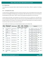
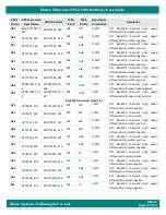
Страница 50: ...S IOs to Board to Board Connector2 Even though Bank66 signals are routed as LVDS IOs these pins can be used as SE IOs if required The Board to Board Connector2 pins 169 170 171 172 176 178 and 177 are...

Страница 51: ...155 PL_AV21_LVDS6 6_L10P_QBC IO_L10P_T1U_N6 _QBC_AD4P_66 66 AV21 IO 1 8V Bank66 IO10 differential positive Same pin can be configured as PLSYSMON differential analog input4 positive or Single ended I...

Страница 52: ...e ended I O 181 PL_BC17_LVDS66 _L5N IO_L5N_T0U_N9_ AD14N_66 66 BC17 IO 1 8V Bank66 IO5 differential negative Same pin can be configured as PLSYSMON differential analog input14 negative or Single ended...

Страница 53: ...igured as PLSYSMON differential analog input8 negative or Single ended I O 140 PL_AL19_LVDS66 _L23P IO_L23P_T3U_N8 _66 66 AL19 IO 1 8V Bank66 IO23 differential positive Same pin can be configured as S...

Страница 54: ...ifferential negative Same pin can be configured as Single ended I O 162 PL_BF19_LVDS66 _L2P IO_L2P_T0L_N2_6 6 66 BF19 IO 1 8V Bank66 IO2 differential positive Same pin can be configured as Single ende...

Страница 55: ...igured as PLSYSMON differential analog input1 positive or Single ended I O IO Type of IOs originating from KU19P FPGA is configurable Hence for exact IO type configuration options refer Xilinx KU19P F...

Страница 56: ...be configured as PLSYSMON differential analog input0 negative or Single ended I O 85 PL_AP13_LVDS67 _L22P_DBC IO_L22P_T3U_N6 _DBC_AD0P_67 67 AP13 IO 1 8V Bank67 IO22 differential positive Same pin ca...

Страница 57: ...sitive or Single ended I O 105 PL_AP14_LVDS67 _L20N IO_L20N_T3L_N3 _AD1N_67 67 AP14 IO 1 8V Bank67 IO29 differential negative Same pin can be configured as PLSYSMON differential analog input1 negative...

Страница 58: ...sitive or Single ended I O 141 PL_BD14_LVDS6 7_L5N IO_L5N_T0U_N9_ AD14N_67 67 BD14 IO 1 8V Bank67 IO5 differential negative Same pin can be configured as PLSYSMON differential analog input14 negative...

Страница 59: ...4_LVDS67 _L16N_QBC IO_L16N_T2U_N7 _QBC_AD3N_67 67 AV14 IO 1 8V Bank67 IO16 differential negative Same pin can be configured as PLSYSMON differential analog input3 negative or Single ended I O 98 PL_AU...

Страница 60: ..._67 67 AW13 IO 1 8V Bank67 IO13 differential negative Same pin can be configured as GC Global Clock differential negative or Single ended I O 116 PL_BA15_LVDS67 _L11P_GC IO_L11P_T1U_N8 _GC_67 67 BA15...

Страница 61: ...he Kintex Ultrascale FPGA SOM supports VRTC_3V0 coin cell power input from Board to Board Connector2 and connected to PMIC s VBBAT pin for real time clock backup voltage For more details on Power pins...

Страница 62: ...ed in the below table and the interfaces which are available at Board to Board Connector3 are explained in the following sections The Board to Board Connector3 J5 is physically located on bottom side...

Страница 63: ...YRXN1_230 B8 GND C8 GTYRXN0_231 D8 GND A9 GTYRXP1_230 B9 GND C9 GTYRXP0_231 D9 GND A10 GND B10 GTYTXN1_230 C10 GND D10 GTYRXP2_228 A11 GND B11 GTYTXP1_230 C11 GND D11 GTYRXN2_228 A12 GTYTXN3_230 B12 G...

Страница 64: ...P1_228 A32 GTYTXP0_229 B32 GND C32 GTYTXN3_231 D32 GND A33 GTYTXN0_229 B33 GND C33 GTYTXP3_231 D33 GND A34 GND B34 GTREFCLK1P_229 C34 GND D34 GTYTXN0_228 A35 GND B35 GTREFCLK1N_229 C35 GND D35 GTYTXP0...

Страница 65: ..._232 D49 GND A50 GND B50 NC C50 GND D50 GTYRXN0_232 A51 GND B51 NC C51 GND D51 GTYRXP0_232 A52 NC B52 GND C52 GTYTXP0_232 D52 GND A53 NC B53 GND C53 GTYTXN0_232 D53 GND A54 GND B54 NC C54 GND D54 GTYT...

Страница 66: ...e below table B2B 3 Pin No B2B Connector3 Signal Name FPGA Pin Name FPGA Bank FPGA Pin No Signal Type Termination Description Bank228 Transceiver Quad Pins D2 B2B_GTREFCLK0 P_228 MGTREFCLK0P_2 28 228...

Страница 67: ...K1P_22 8 MGTREFCLK1P_2 28 228 AF11 I DIFF GTY Bank228 channel1 High speed differential reference clock1 positive Bank229 Transceiver Quad Pins A24 GTYRXN2_229 MGTYRXN2_229 229 W3 I DIFF GTY Bank229 ch...

Страница 68: ...9 MGTREFCLK0N_ 229 229 Y10 I DIFF GTY Bank229 channel0 High speed differential reference clock0 negative Bank230 Transceiver Quad Pins A4 GTYRXN0_230 MGTYRXN0_230 230 U3 I DIFF GTY Bank230 channel0 H...

Страница 69: ...F GTY Bank230 channel0 High speed differential reference clock0 positive Bank231 Transceiver Quad Pins C4 GTYRXP2_231 MGTYRXP2_231 231 L4 I DIFF GTY Bank231 channel2 High speed differential receiver p...

Страница 70: ...nnel0 High speed differential receiver positive Bank232 Transceiver Quad Pins A1 GTREFCLK1N_23 2 MGTREFCLK1N_ 232 232 F10 I DIFF GTY Bank232 channel1 High speed differential reference clock1 negative...

Страница 71: ...igh speed differential receiver positive D54 GTYTXP2_232 MGTYTXP2_232 232 G9 O DIFF GTY Bank232 channel2 High speed differential transmitter positive D55 GTYTXN2_232 MGTYTXN2_232 232 G8 O DIFF GTY Ban...

Страница 72: ...22 A23 A26 A27 A30 A31 A34 A35 A38 A39 A42 A43 A46 A47 A50 A51 A54 A55 A58 B1 B4 B5 B8 B9 B12 B13 B16 B17 B20 B21 B24 B25 B28 B29 B32 B33 B36 B37 B40 B41 B44 B45 B48 B49 B52 B53 B56 B57 B60 C2 C3 C6 C...

Страница 73: ...ded in the below table and the interfaces which are available at Board to Board Connector4 are explained in the following sections The Board to Board Connector4 J4 is physically located on bottom side...

Страница 74: ...5 GND B5 GTYRXP3_227 C5 GND D5 NC A6 GTREFCLK0P_227 B6 GND C6 NC D6 GND A7 GTREFCLK0N_227 B7 GND C7 NC D7 GND A8 GND B8 GTYRXN2_227 C8 GND D8 NC A9 GND B9 GTYRXP2_227 C9 GND D9 NC A10 GTYTXP0_227 B10...

Страница 75: ...227 MGTREFCLK0N_ 227 227 AM10 I DIFF GTY Bank227 channel0 High speed differential reference clock0 negative A10 GTYTXP0_227 MGTYTXP0_227 227 AN9 O DIFF GTY Bank227 channel0 High speed differential tra...

Страница 76: ...6 GTYRXN0_227 MGTYRXN0_227 227 AN3 I DIFF GTY Bank227 channel0 High speed differential transmitter negative B17 GTYRXP0_227 MGTYRXP0_227 227 AN4 I DIFF GTY Bank227 channel0 High speed differential tra...

Страница 77: ...Function 7 Function 8 Integrated Flash Controller NA IFC_A16 QSPI_CS_A0 IFC_A16 QSPI_CS_A0 NA IFC_A17 QSPI_CS_A1 IFC_A17 QSPI_CS_A1 NA IFC_A18 QSPI_CK_A IFC_A18 QSPI_CK_A NA IFC_A19 QSPI_CS_B0 IFC_A1...

Страница 78: ...1_PC S5 IFC_AD12 SPI1_PCS5 cfg_rcw_src4 NA IFC_AD13 cfg_rcw_src5 SPI1_SO UT IFC_AD13 SPI1_SOUT cfg_rcw_src5 NA IFC_AD14 cfg_rcw_src6 IFC_AD14 cfg_rcw_src6 NA IFC_AD15 cfg_rcw_src7 IFC_AD15 cfg_rcw_src...

Страница 79: ...X_BCLK EC1_TX_CLK FTM1_EXTCLK NA EC1_GTX_CLK125 GPIO3_08 EC1_RX_ER EXT_AUDIO_MCLK2 EC1_GTX_CLK12 5 GPIO3_08 EXT_AUDIO_ MCLK2 EC1_RX_ER NA EC1_RX_CLK GPIO3_13 SAI1_RX_BCLK FTM1_QD_PHA EC1_RX_CLK GPIO3_...

Страница 80: ...1588_CLK _IN FTM3_QD_PH A NA EC3_RX_DV GPIO4_08 TSEC_1588_TRIG_IN1 FTM3_QD_PHB EC3_RX_DV GPIO4_08 TSEC_1588_TRI G_IN1 FTM3_QD_PH B NA EC3_RXD0 GPIO4_06 TSEC_1588_TRIG_IN2 EC2_CRS FTM3_CH2 EC3_RXD0 GPI...

Страница 81: ...SDHC_DAT3 GPIO2_08 LPUART6_SOU T LPUART3_RTS_B SPI2 NA UART1_CTS_B GPIO1_21 UART3_SIN LPUART2_SIN SPI2_SIN 2D ACE_VSYNC UART1_CTS_B GPIO1_21 LPUART2_SIN UART3_SIN SPI2_SIN 2D ACE_VSYNC NA UART1_RTS_B...

Страница 82: ...FTM4_QD_PHB NA CLK11 GPIO4_21 BRGO4 SAI4_RX_SYNC FTM8_CH0 2D ACE_DE CLK11 GPIO4_21 BRGO4 SAI4_RX_SYNC 2D ACE_DE FTM8_CH0 NA CLK12 GPIO4_22 BRGO1 FTM8_CH1 2DACE_ CLK_OUT CLK12 GPIO4_22 BRGO1 2D ACE_CL...

Страница 83: ...4_28 SPI2_PCS4 SDHC_WP LPUART 50 SDHC_CMD GPIO2_04 LPUART3_SOUT SDHC_CMD GPIO2_04 LPUART3_SOU T 52 SDHC_DAT0 GPIO2_05 LPUART3_SIN SDHC_DAT0 GPIO2_05 LPUART3_SIN 81 SDHC_DAT1 GPIO2_06 LPUART2_RTS_B LPU...

Страница 84: ...C GPIO4_12 UC1_RTSB_TXE N SAI3_TX_SYNC 2D ACE_D03 FTM4_CH4 69 TDMB_RQ GPIO4_18 UC3_CDB_RXER SPDIF_EXTCLK SAI4_RX_BCLK FTM4_EXTCLK 2D ACE_D09 TDMB_RQ GPIO4_18 SPDIF_EXTCLK UC3_CDB_RXER SAI4_RX_BCLK 2D...

Страница 85: ...er Input Requirement The below table provides the Power Input Requirement of Kintex Ultrascale FPGA KU19P SOM Table 8 Power Input Requirement Sl No Power Rail Min V Typical V Max V Max Input Ripple 1...

Страница 86: ...Connector1 must be low at the same time or before VCC_5V goes down VCC_5V must go down at the same time or before VRTC_3V0 goes down Figure 9 Power Input Sequencing Table 9 Power Sequence Timing Item...

Страница 87: ...REL0 1 Page 87 of 95 Kintex Ultrascale FPGA KU19P SOM Hardware User Guide iWave Systems Technologies Pvt Ltd 3 1 3 Power Consumption TBD...

Страница 88: ...ystem enclosure air circulation in the system system power supply etc Based on the system design specific heat dissipating approach might be required from system to system It is recommended to do the...

Страница 89: ...size is decreasing and performance of module is increasing by rising processor frequencies it generates high amount of heat which should be dissipated for the system to work as expected without fault...

Страница 90: ...ogies Pvt Ltd 3 3 Mechanical Characteristics 3 3 1 Kintex Ultrascale FPGA SOM Mechanical Dimensions Kintex Ultrascale FPGA KU19P SOM PCB size is 110mm x 75mm x 2 64mm and weight is 125g SOM mechanical...

Страница 91: ...e FPGA SOM Bottom View Kintex Ultrascale FPGA KU19P PCB thickness is 2 64mm 0 1mm top side maximum height component is Inductors L1 L2 L3 6mm and bottom side maximum height component is Board to Board...

Страница 92: ...REL0 1 Page 92 of 95 Kintex Ultrascale FPGA KU19P SOM Hardware User Guide iWave Systems Technologies Pvt Ltd Figure 13 Mechanical dimension of Kintex Ultrascale FPGA SOM Side View...

Страница 93: ...ifferent Kintex Ultrascale FPGA KU19P SOM variations Please contact iWave for orderable part number of higher RAM memory size or Flash memory size SOM configurations Also if the desired part number is...

Страница 94: ...trascale FPGA SOM Development Platform which is targeted for quick validation of Kintex Ultrascale FPGA KU19P based SOM iWave s Kintex Ultrascale FPGA Development Board incorporates Kintex Ultrascale...

Страница 95: ...REL0 1 Page 95 of 95 Kintex Ultrascale FPGA KU19P SOM Hardware User Guide iWave Systems Technologies Pvt Ltd...

Отзывы: