REL0.1
Page 48 of 95
Kintex Ult FPGA SOM Hardware User Guide
iWave Systems Technologies Pvt. Ltd.
2.8.1.6
JTAG Interface
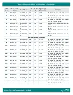
The Kintex Ult FPGA SOM supports JTAG interface on Board-to-Board Connector2. Both LS1021A and KU19P share a
common set of JTAG pins in the Board-to-Board2 connector and each have their own TAP controller.
KU19P and LS1021A’s JTAG
signals are given to JTAG Selection 2:1 Mux IC which will select according to JTAG_SEL configuration.
Refer the below table for JTAG selection details.
JTAG_SEL
JTAG Controller
0
LS1021A
1
KU19P
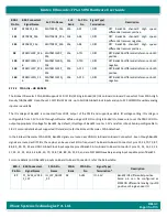
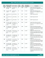
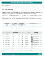
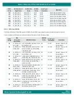
By default, the JTAG_SEL will be high and KU19P will be selected as JTAG controller. Refer the below given pinout for more details.
B2B-2
Pin No
B2B Connector2
Signal Name
FPGA Pin Name
FPGA
Bank
FPGA
Pin No
Signal Type/
Termination
Description
27
JTAG_TDI
TDI_0
0
AE15
I, 1.8V LVCMOS/
4.7K
JTAG Test Data Input.
29
JTAG_TMS
TMS_0
0
AG15
I, 1.8V LVCMOS/
4.7K
JTAG Test Mode Select.
31
JTAG_TCK
TCK_0
0
AE13
I, 1.8V LVCMOS/
4.7K
JTAG Test Clock.
33
JTAG_TDO
TDO_0
0
AC13
O, 1.8V LVCMOS
JTAG Test Data Output.
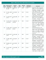
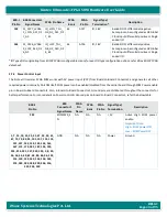
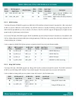
If the JTAG_SEL pin is low it will select LS1021A as JTAG controller. Refer the below pinout for more details.
B2B-2
Pin No
B2B Connector2
Signal Name
LS1021A Pin
Name
LS1021A
Pin No
Signal Type/
Termination
Description
25
LS_JTAG_TRST
TRST_B
F6
I, 1.8V LVCMOS
JTAG Test Reset from LS1021A
27
JTAG_TDI
TDI
E7
I, 1.8V LVCMOS/
4.7K
JTAG Test Data Input.
29
JTAG_TMS
TMS
F8
I, 1.8V LVCMOS/
4.7K
JTAG Test Mode Select.
31
JTAG_TCK
TCK
E8
I, 1.8V LVCMOS/
4.7K
JTAG Test Clock.
33
JTAG_TDO
TDO
F7
O, 1.8V LVCMOS
JTAG Test Data Output.
2.8.1.7
SerDes Interface
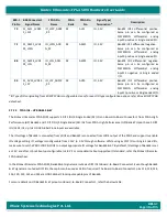
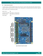
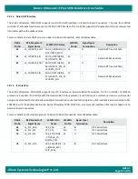
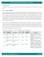
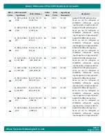
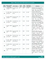
The Kintex Ult FPGA SOM supports 2 highspeed SerDes lanes through LS1021A Layerscape Processor in board-to-board
connector2
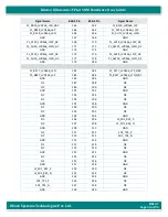
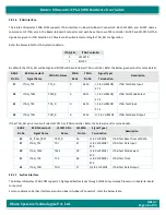
For more details on SerDes Interface pinouts on Board-to-Board Connector2, refer the below table.

