REL0.1
Page 32 of 95
Kintex Ult FPGA SOM Hardware User Guide
iWave Systems Technologies Pvt. Ltd.
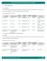
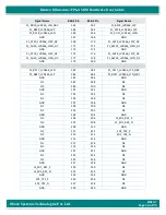
B2B-2
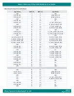
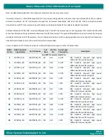
Pin No
B2B Connector1
Signal Name
LS1021A Pin
Name
LS1021A
Pin No
Signal Type/
Termination
Description
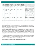
18
LS_GPIO3_22(EC2_R
XD3)
EC2_RXD3/GPI
O3_22/CAN4_
RX/USB2_D3/F
TM2_CH4
R2
O, 3V3
General
Purpose
I/O
from
LS1021A Processor
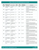
28
LS_GPIO3_18(EC2_T
XD0)
EC2_TXD0/GPI
O3_18/USB2_
D4/FTM2_CH2
T3
I, 3V3
General
Purpose
I/O
from
LS1021A Processor
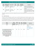
30
LS_GPIO3_17(EC2_T
XD1)
EC2_TXD1/GPI
O3_17/USB2_
D5/FTM2_CH3
T4
I, 3V3
General
Purpose
I/O
from
LS1021A Processor
32
LS_GPIO3_24(EC2_R
XD1)
EC2_RXD1/GPI
O3_24/USB2_
D1/FTM2_CH1
U1
I, 3V3
General
Purpose
I/O
from
LS1021A Processor
34
LS_GPIO4_09(TDMA
_RXD)
TDMA_RXD/G
PIO4_09/UC1_
RXD7/SAI3_RX
_DATA/FTM4_
CH7/2D-
ACE_D00
H3
I, 3V3
General
Purpose
I/O
from
LS1021A Processor
38
LS_GPIO3_19(EC2_T
XEN)
EC2_TX_EN/GP
IO3_19/USB2_
STP/FTM2_FA
ULT
T5
O, 3V3
General
Purpose
I/O
from
LS1021A Processor
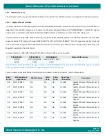
2.7.2
FPGA Interfaces
The interfaces which are supported in Board-to-Board Connector1 from Kintex Ult FPGA is explained in the following
section.
2.7.2.1
GTY High Speed Transceivers
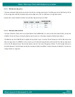
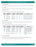
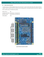
The Kintex Ult FPGA (KU19P) supports 32 GTY transceivers through 8 transceiver Quad (Bank 225, 226, 228, 229, 230, 231,
232 & 227) with line rate from 500Mbps to 32.75Gbps based on the speed grade of the FPGA. These transceivers can be used to
interface to multiple high-speed interface protocols. Each GTY transceiver quad supports two dedicated reference clock input pairs.
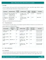
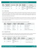
Kintex Ult FPGA
Speed Grade
GTY Transceiver line rate
(min)
GTY Transceiver line rate
(max)
-1L Speed Grade
0.5Gbps
12.5 Gbps
-1 Speed Grade
0.5 Gbps
25.785 Gbps
-2 Speed Grade
0.5 Gbps
28.21 Gbps
-3 Speed Grade
0.5 Gbps
32.75 Gbps

