REL0.1
Page 14 of 95
Kintex Ult FPGA SOM Hardware User Guide
iWave Systems Technologies Pvt. Ltd.
2.3
Kintex Ult FPGA
2.3.1
FPGA & Design Information
The Kintex Ult FPGA SoC provides best performance with up to 40% lower power than previous generation Kintex series
due to enhanced system logic cell packaging. This also includes the highest signal processing bandwidth in a mid-range device, next
generation transceivers. The family is ideal for DSP intensive processing required for next generation and packet processing in 100G
networking.
Note: Please refer the latest Kintex Ult FPGA Datasheet & Technical Reference Manual for more details which may be revised
from time to time.
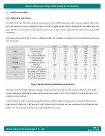
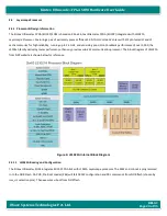
Figure 2: Kintex Ult FPGA Devices Comparison
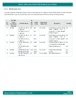
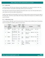
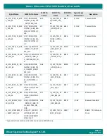
The Kintex Ult FPGA’s IO Banks are classified as high
-performance (HP) banks or high-density (HD) banks. The HP Bank
I/Os are optimized for highest performance operation organized in banks of 52pins. The HD Bank I/Os are reduced-feature I/Os
organized in banks of 24pins.
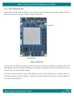
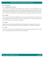
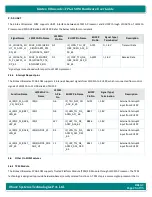
In Kintex Ult FPGA, each IO bank supports four global clock (GC or HDGC) input pin pairs. GC pins have direct access to
the global clock buffers, PLLs of the same Bank. HDGC pins are from HD I/O banks and have direct access only to the global clock
buffers. Also, Kintex Ult FPGA supports high speed GTY transceivers.


