REL0.1
Page 55 of 95
Kintex Ult FPGA SOM Hardware User Guide
iWave Systems Technologies Pvt. Ltd.
B2B-2
Pin No
B2B Connector2
Signal Name
FPGA Pin Name
FPGA
Bank
FPGA
Pin No
Signal Type/
Termination*
Description
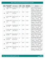
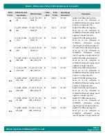
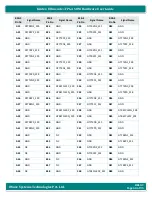
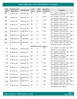
178
PL_AW18_LVDS6
6_L11N_GC
IO_L11N_T1U_N9
_GC_66
66
AW18
IO, 1.8V
Bank66 IO11 differential negative
Same pin can be configured as GC
Global Clock Input differential
negative or Single ended I/O.
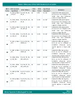
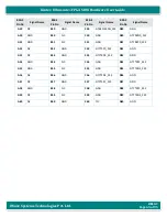
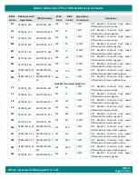
182
PL_AY17_LVDS66
_L7P_QBC
IO_L7P_T1L_N0_Q
BC_AD13P_66
66
AY17
IO, 1.8V
Bank66 IO7 differential positive.
Same pin can be configured as
PLSYSMON
differential
analog
input13 positive or Single ended I/O.
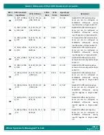
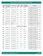
184
PL_BA17_LVDS66
_L7N_QBC
IO_L7N_T1L_N1_
QBC_AD13N_66
66
BA17
IO, 1.8V
Bank66 IO7 differential negative.
Same pin can be configured as
PLSYSMON
differential
analog
input13 negative or Single ended
I/O.
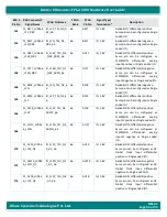
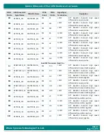
40
PL_AP28_LVDS65
_L20N_D09
IO_L20N_T3L_N3_
AD1N_D09_65
65
AP28
IO, 1.8V
Bank65 IO20 differential negative.
Same pin can be configured as
PLSYSMON
differential
analog
input1 negative or Single ended I/O.
63
PL_AN28_LVDS6
5_L20P_D08
IO_L20P_T3L_N2_
AD1P_D08_65
65
AN28
IO, 1.8V
Bank65 IO20 differential positive.
Same pin can be configured as
PLSYSMON
differential
analog
input1 positive or Single ended I/O.
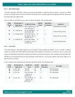
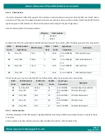
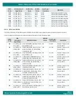
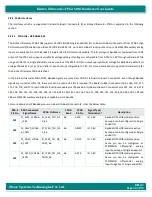
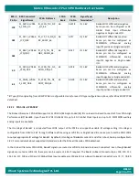
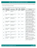
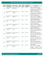
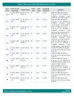
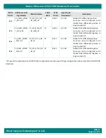
*IO Type of IOs originating from KU19P FPGA is configurable. Hence for exact IO type configuration options, refer Xilinx KU19P FPGA
datasheet.
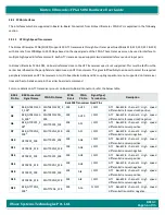
2.8.2.2
FPGA IOs
–
HP BANK67
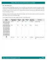
The Kintex Ult FPGA SOM supports 22 LVDS IOs/44 Single Ended (SE) IOs on Board-to-Board Connector2 from FPGA High
Performance (HP) Bank68. Upon these 22 LVDS IOs/44 SE IOs, up to 4 GC Global Clock Inputs and up to 15 PLSYSMON auxiliary
analog inputs are available.
The IO voltage of Bank67 is connected from LDO4 output of the PMIC and supports variable IO voltage setting. IO voltage is
configurable from 0.95V to 1.8V through software. While using as LVDS IOs or Single Ended IOs, make sure to set the PMIC LDO4
to output appropriate IO voltage for Bank67. By default, IO voltage of Bank68 is set as 1V and after U-boot bootup configurable to
1.8V. For more details about supported IO standard, refer the Kintex Ult FPGA datasheet.
In the Kintex Ult FPGA SOM, Bank67 signals are routed as LVDS IOs to Board-to-Board Connector2. Even though Bank67
signals are routed as LVDS IOs, these pins can be used as SE IOs if required. The Board-to-Board Connector2 pins 109, 110, 111,
115, 116, 117, 118 and 110 are GC Global Clock Input capable pins of Bank67. Also, Board to Board Connector2 pins 75, 77, 78, 80,

