REL0.1
Page 8 of 95
Kintex Ult FPGA SOM Hardware User Guide
iWave Systems Technologies Pvt. Ltd.
1.
INTRODUCTION
1.1
Purpose
This document is the Hardware User Guide for the Kintex Ult FPGA System on Module based on the Xilinx Kintex Ult
FPGA (KU19P). This board is fully supported by iWave Systems Technologies Pvt. Ltd. This Guide provides detailed information on
the overall design and usage of the Kintex Ult FPGA System on Module from a Hardware Systems perspective.
1.2
SOM Overview
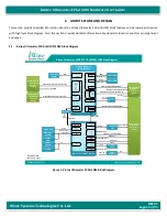
The Kintex Ult FPGA (KU19P) SOM is
integrated with Xilinx KU19P FPGA SoC and NXP’s LS1021A Layerscape Processor
.
Kintex Ult FPGA SOM has a form factor of 110mm x 75mm and provides the functional requirements for an embedded
application. Two high speed ruggedized terminal strip connectors and Two High-Speed High-Density connectors provide the carrier
board interface to carry all the I/O signals to and from the Kintex Ult FPGA SOM.
1.3
List of Acronyms
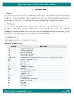
The following acronyms will be used throughout this document.
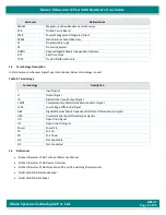
Table 1: Acronyms & Abbreviations
Acronyms
Abbreviations
ADC
Analog to Digital Converter
ARM
Advanced RISC Machine
BSP
Board Support Package
RCW
Reset Configuration Word
CPU
Central Processing Unit
DDR4 SDRAM
Double Data Rate fourth-generation Synchronous Dynamic Random Access Memory
FPGA
Field Programmable Gate Array
PBL
Pre-boot Loader
GB
Giga Byte
Gbps
Gigabits per sec
IFC
Integrated Flash Controller
GHz
Giga Hertz
GPIO
General Purpose Input Output
I2C
Inter-Integrated Circuit
IC
Integrated Circuit
JTAG
Joint Test Action Group
Kbps
Kilobits per second
LVDS
Low Voltage Differential Signalling
MAC
Media Access Controller
MB
Mega Byte
Mbps
Megabits per sec
MHz
Mega Hertz


