


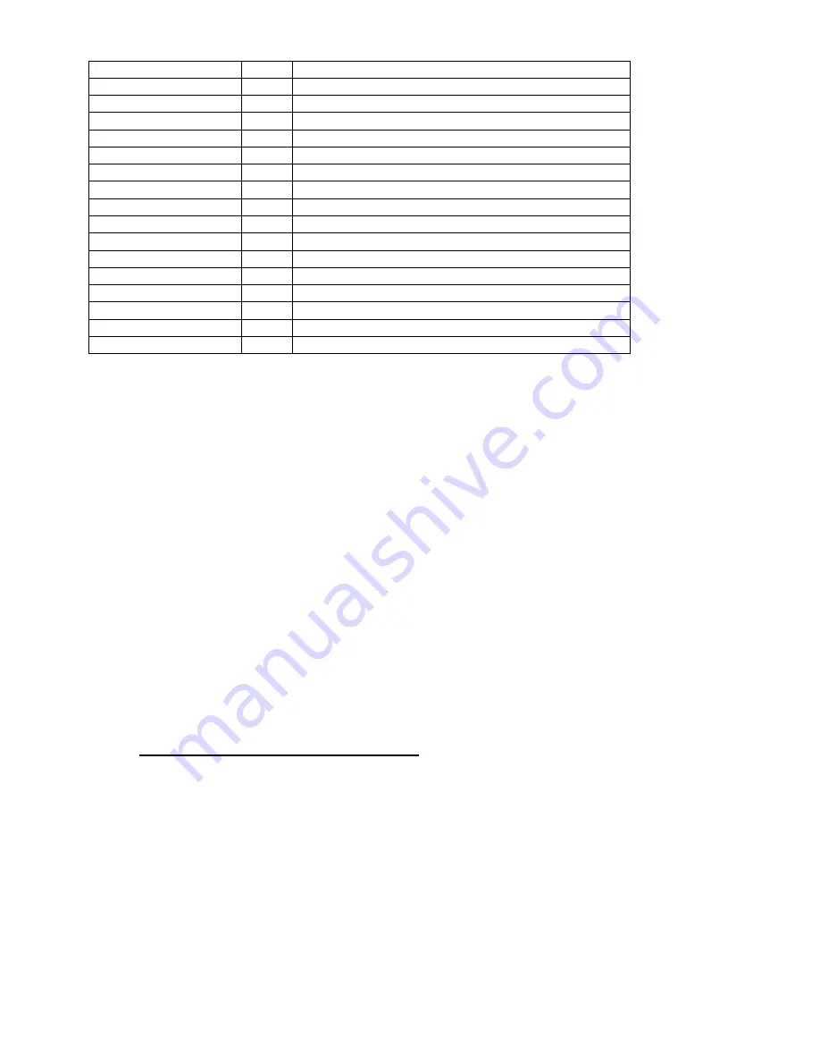
20
40
2 ROI Start Line
42
2 ROI End Line
44
2 Line Period in Pixel Clocks
46
4 Exposure Time in Pixel Clocks
50
4 Frame Period in Pixel Clocks
54
4 Exposure Delay in Pixel Clocks
58
2 Serial Link Bit Period in Pixel Clocks
60
1 Camera Link Readout Mode
61
1 Camera Link Clock Frequency
62 1
Binning
63 1
Memory
Options
64
1 Sensor Resolution - 8/10 bit
65
2 Trigger Mode (2
nd
Byte is Data FPGA dependent)
67
1 Frame count for Multi-Trigger mode
68
1 CC Mode: CC2, CC3, CC4 enable and edge select
69
59 Reserved for Control FPGA / base system extension
128
384 Available for Data FPGA functionality extensions
Table 4 - Camera State Memory Layout
Sensor reference voltages are presented to the DAC’s exactly as they are stored in the state. The order
listed above is the recommended order, but other orders may work. The format for these is MS byte first
with the most significant nibble indicating the command code to the DAC. Pairs of values are sent, one to
each DAC chip with the first going to U25 and the second to U26. Voltages are updated in the order sent.
Default values shown are for the FastCamera 13. For more information see the LTC1660 data sheet.
Whenever the state memory is updated from host or flash, the actual internal registers that implement the
camera state change, too. Some of these are located in the Control FPGA and some in the Data FPGA.
The Control FPGA forwards state data to the Data FPGA whenever it is updated.
The state memory holds all of the state variables currently defined for camera operational modes as well as
some additional storage that can be defined as required for more sophisticated Data FPGAs. The Data
FPGAs can count on this storage to be refreshed from flash after initial FPGA load and whenever the user
restores state from one of the saved sets in flash.
In addition to the camera state storage pages, some of the flash memory is available for Data FPGA
storage requirements such as pixel defect maps. The amount of flash available for this depends on the
size of the Data FPGA and the size of the flash device. A pointer in the flash header in page zero indicates
the starting page of the Data FPGA initialization area. Its length in pages (which may be zero) is stored in
the flash header as well. Data from this initialization area is read out and sent to the data FPGA after initial
FPGA load. Although the data in these pages has no predefined layout, the first page must start with the
sequence 3C, A5, 0F, 96. This prevents transmission of uninitialized flash pages and serves to identify the
following data as Data FPGA Initialization Data rather than Camera State.
16. SERIAL CONTROL INTERFACE
Содержание FastCamera13
Страница 1: ...FASTCAMERA SERIES FASTCAMERA13 USER S MANUAL FVM 50013...
Страница 32: ...32...