background image


Document type: 

Title: 

Revision date: 

Revision: 

User's Manual (MUT) 

 Mod. V1724 8 Channel 14bit - 100MS/s Digitizer 

06/11/2007 


NPO: 

Filename: 

Number of pages: 

Page: 

00103/05:V1724x.MUTx/07 V1724_REV7.DOC 

63 

57 


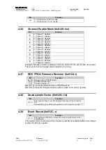
4.30. 

Set Monitor DAC (0x8138; r/w) 

Bit 

Function 

[11:0]  This register allows to set the DAC value (12bit) 

This register 

allows to set the DAC value

 in Voltage level mode (see § 2.7).  

LSB = 0.244 mV, terminated on 50 Ohm. 

4.31. 

Board Info (0x8140; r) 

Bit 

Function 

[15:8]  Memory size (Mbyte/channel) 

[7:0] 

Board Type: 
0 = V1724 

4.32. Monitor 

Mode 

(0x8144; 

r/w) 

Bit 

Function 

[2:0] 

This register allows to encode the Analog Monitor (see § 3.7) operation: 
000 = Trigger Majority Mode 
001 = Test Mode 
010 = Analog Monitor/Inspection Mode 
011 = Buffer Occupancy Mode 
100 = Voltage Level Mode 

4.33. 

Event Size (0x814C; r) 

Bit 

Function 

[31:0]  Nr. of 32 bit words in the next event 

4.34. 

Analog Monitor (0x8150; r/w) 

Bit 

Function 

[21,20]

Magnify factor: 
00 = 1x  
01 = 2x 
10 = 4x 
11 = 8x 

[19] 

Offset sign (0=positive; 1=negative) 

[18:8] Offset 

Value 

[7] 

0 = Channel 7  disabled 
1 = Channel 7  enabled 

[6] 

0 = Channel 6  disabled 
1 = Channel 6  enabled 

[5] 

0 = Channel 5  disabled 
1 = Channel 5  enabled 

[4] 

0 = Channel 4  disabled 
1 = Channel 4  enabled 

[3] 

0 = Channel 3  disabled 
1 = Channel 3  enabled 

[2] 

0 = Channel 2  disabled 
1 = Channel 2  enabled 

[1] 

0 = Channel 1  disabled 
1 = Channel 1  enabled 

[0] 

0 = Channel 0  disabled 

Содержание V1724 Series

Страница 1: ...Technical Information Manual MOD V1724 6 November 2007 Revision n 7 8 CHANNEL 14 BIT 100 MS S DIGITIZER MANUAL REV 7 NPO 00103 05 V1724x MUTx 07...

Страница 2: ...responsibility for damages or injuries caused by an improper use of the Modules due to negligence on behalf of the User It is strongly recommended to read thoroughly the CAEN User s Manual before any...

Страница 3: ...plays 13 2 6 INTERNAL COMPONENTS 13 2 7 TECHNICAL SPECIFICATIONS TABLE 15 3 FUNCTIONAL DESCRIPTION 16 3 1 ANALOG INPUT 16 3 1 1 Single ended input 16 3 1 2 Differential input 16 3 2 CLOCK DISTRIBUTION...

Страница 4: ...Mode 2 33 3 7 3 1 Procedure to enable Analog Monitor mode 34 3 7 3 2 Applications examples 34 3 7 4 Buffer Occupancy Mode Monitor Mode 3 35 3 7 5 Voltage Level Mode Monitor Mode 4 35 3 8 TEST PATTERN...

Страница 5: ...FPGA FIRMWARE 0X1N8C R 50 4 9 CHANNEL N BUFFER OCCUPANCY 0X1N94 R 51 4 10 CHANNEL N DAC REGISTER 0X1N98 R W 51 4 11 CHANNEL N ADC CONFIGURATION 0X1N9C R W 51 4 12 CHANNEL CONFIGURATION 0X8000 R W 51...

Страница 6: ...4 42 BLT EVENT NUMBER 0XEF1C R W 59 4 43 SCRATCH 0XEF20 R W 59 4 44 SOFTWARE RESET 0XEF24 W 59 4 45 SOFTWARE CLEAR 0XEF28 W 59 4 46 FLASH ENABLE 0XEF2C R W 59 4 47 FLASH DATA 0XEF30 R W 60 5 INSTALLA...

Страница 7: ...3 16 INSPECTION MODE DIAGRAM 33 FIG 3 17 EXAMPLE OF MAGNIFY PARAMETER USE ON SINGLE CHANNEL 34 FIG 3 18 EXAMPLE OF MAGNIFY AND OFFSET PARAMETERS USE ON SINGLE CHANNEL 35 FIG 3 19 A24 ADDRESSING 37 FI...

Страница 8: ...ended 4 Msamples ch Yes EP1C20 6U VME64X VX1724F Differential 4 Msamples ch Yes EP1C20 6U VME64X AMC ADC e Memory controller FPGA Models available ALTERA Cyclone EP1C4 4000 Logic elements or ALTERA C...

Страница 9: ...ee Accessories Controller The V1724 can be controlled and readout through the Optical Link in parallel to the VME interface The Mod V1724LC is also available a simplified version of the Mod V1724 with...

Страница 10: ...10 2 Technical specifications 2 1 Packaging The module is housed in a 6U high 1U wide VME unit The board hosts the VME P1 and P2 connectors and fits into both VME VME64 standard and V430 backplanes VX...

Страница 11: ...Filename Number of pages Page 00103 05 V1724x MUTx 07 V1724_REV7 DOC 63 11 2 3 Front Panel SCALER 8 CH 14 BIT 100 MS S DIGITIZER Mod V560E Mod V1724 ANALOG INPUT DIGITAL I O s ANALOG MONITOR OUTPUT L...

Страница 12: ...chanical specifications Tyco MODU II N B absolute max analog input voltage 6Vpp with Vrail max to 6V or 6V for any DAC offset value 2 4 2 CONTROL connectors Function TRG OUT Local trigger output NIM T...

Страница 13: ...me Colour Function DTACK green VME read write access to the board CLK_IN green External clock enabled NIM green Standard selection for CLK I O V1724LC Rev 0 TRG OUT TRG IN S IN TTL green Standard sele...

Страница 14: ...T Mod V1724 8 Channel 14bit 100MS s Digitizer 06 11 2007 7 NPO Filename Number of pages Page 00103 05 V1724x MUTx 07 V1724_REV7 DOC 63 14 y y y y ROTARY SWITCHES SW2 5 BASE ADDRESS 31 16 CLK SOURCE SW...

Страница 15: ...ent size and pre post trigger Divisible into 1 1024 buffers Trigger Common External TRGIN NIM or TTL and VME Command Individual channel autotrigger time over under threshold TRGOUT NIM or TTL for the...

Страница 16: ...125V 5V with high range input DC offset in order to preserve the full dynamic range also with unipolar positive or negative input signals The input bandwidth ranges from DC to 40 MHz with 2nd order l...

Страница 17: ...trigger through a clock chain Such domain can use either an external via front panel signal or an internal via local oscillator source selection is performed via dip switch SW1 see 2 6 in the latter...

Страница 18: ...acquisition window 3 2 4 Output Clock Front panel Clock Output is User programmable Odiv and Odel parameters allows to obtain a signal with the desired frequency and phase shift in order to recover c...

Страница 19: ...e shift delay in Output Clock field of CAENPLLConfig Main menu the tool refuses wrong settings for such parameters 3 2 7 Direct Drive programming In Direct Drive BYPASS mode the User can directly set...

Страница 20: ...delivers the 100 MHz Sampling Clock to the ADCs The 100 MHz Sampling Clock is fed also to the FPGA ROC in order to allow trigger synchronisation see also Fig 1 1 and to CLK_OUT processed by a programm...

Страница 21: ...e validated by the S_IN signal otherwise they are rejected data storage takes place by couples of samples two 32 bit long words per time Two operating modes are foreseen as decrbed in the following 3...

Страница 22: ...48 S52 D1 D1 D1 D1 D1 D5 D1 D5 D1 D5 D1 D5 D1 D5 D9 D1 D5 D9 D1 D5 D9 MEMORY BUFFER D1 D5 D9 Fig 3 6 Data storage2 in Sample Mode 3 3 4 Acquisition Triggering Samples and Events When the acquisition i...

Страница 23: ...red number of samples for building the pre trigger of the event is not reached yet this happens typically as the trigger occurs too early either with respect to the RUN_ACQUISITION command see 3 3 1 o...

Страница 24: ...N 1 CH 0 SAMPLE N 2 CH 0 SAMPLE 1 CH 1 SAMPLE 0 CH 1 SAMPLE 3 CH 1 SAMPLE 2 CH 1 SAMPLE N 1 CH 1 SAMPLE N 2 CH 1 HEADER DATA CH0 DATA CH1 SAMPLE 1 CH 7 SAMPLE 0 CH 7 SAMPLE 3 CH 7 SAMPLE 2 CH 7 SAMPL...

Страница 25: ...place via two more registers CHANNEL n ZS_THRES and CHANNEL n ZS_NSAMP It must be noticed that one datum 32 bit long word contains 2 samples therefore one datum is considered over threshold as at lea...

Страница 26: ...Total size totale of the event total number of transferred data Control word stored valid data if control word is good Control word stored valid data if control word is good The total size is the num...

Страница 27: ...th positive logic and non overlapping NLBK NLFWD then the readout event is N 2 N 4 5 control words 1 size Skip N1 NLBK Good N 2 NLBK N2 NLFWD N 2 words with samples over threshold Skip N3 NLFWD NLBK G...

Страница 28: ...N5 N 5 words with samples under threshold In some cases the number of data to be discarded can be smaller than NLBK and NLFWD 1 If the algorithm works in positive logic and N1 NLBK N3 NLFWD 0 Fig 3 11...

Страница 29: ...ords 1 size Skip N1 Good N 2 N2 N3 N4 NLFWD N 2 words with samples over threshold Skip N5 NLFWD 4 If the algorithm works in positive logic and N3 NLBK N1 NLFWD 0 Fig 3 12 Example with positive logic a...

Страница 30: ...trigger this means that all the channels store an event at the same time and in the same way same number of samples and same position with respect to the trigger several trigger sources are available...

Страница 31: ...s see 3 5 4 CH0 IN THRESHOLD Local Trigger CH0 Channel Configuration register 6 0 Nth 4samples Nth 4samples Nth 4samples Local Trigger CH0 Channel Configuration register 6 1 Fig 3 14 Local trigger gen...

Страница 32: ...Fig 1 1 whose input is controlled by the ROC FPGA and the signal output driving 50 Ohm is available on the MON output connector MON output of more boards can be summed by an external Linear Fan In Thi...

Страница 33: ...er 0 In this mode the MON output provides a signal whose amplitude is proportional to the number of channels over the trigger threshold The amplitude step 1 channel over threshold is 125mV 3 7 2 Test...

Страница 34: ...nd drives 50 Ohm 3 7 3 1 Procedure to enable Analog Monitor mode In order to enable Analog Monitor mode is necessary to enable the channels to send data to FPGA ROC by setting to 1 bit 7 of Channel Co...

Страница 35: ...DAC produces a copy of the signal on channel 0 with 125 mV dynamics 1 8 of DAC dynamics and 500 mV average value If a larger dynamics is desired it is necessary to modify 0FFSET and MAGNIFY factor in...

Страница 36: ...clears the data off the Output Buffer The Memory Reset can be forwarded via either a write access to Software Clear Register see 4 45 or with a pulse sent to the front panel Memory Clear input see 3 6...

Страница 37: ...only with either a Power ON cycle or a System Reset see 3 8 3 10 1 2 CR CSR address GEO address is picked up from relevant backplane lines and written onto bit 23 19 of CR CSR space indicating the sl...

Страница 38: ...Once an event is completed the relevant memory buffer becomes free and ready to be written again old data are lost After the last word in an event the first word Header of the subsequent event is rea...

Страница 39: ...such cycles Several contiguous boards in order to be daisy chained must be configured as first intermediate or last via MCST Base Address and Control Register see 4 38 A common Base Address is then d...

Страница 40: ...ta at 80 MB s therefore it is possible to connect up to eight V1724 64 ADC channels to a single Optical Link Controller a standard PC equipped with the PCI card CAEN Mod A2818 The A2818 is a 32 bit 33...

Страница 41: ...b for Microsoft Visual C 6 0 Linux dynamic library CAENVMELib is logically located between an application like the samples provided and the device driver The following sections describe the CAENVMELib...

Страница 42: ...An error code about the execution of the function Description The function performs a single VME read cycle CAENVME_API CAENVME_ReadCycle long Handle unsigned long Address void Data CVAddressModifier...

Страница 43: ...en to the VME bus in AM An array of address modifiers in DW An array of data widths Returns An array of error codes about the execution of the function Description The function performs a sequence of...

Страница 44: ...ycle int32_t Handle uint32_t Address void Buffer int Size CVAddressModifier AM CVDataWidth DW int count 3 13 9 CAENVME_MBLTReadCycle Parameters in Handle The handle that identifies the device in Addre...

Страница 45: ...Returns An error code about the execution of the function Description The function returns a bit mask indicating the active IRQ lines CAENVME_API CAENVME_IRQCheck long Handle byte Mask 3 13 12 CAENVME...

Страница 46: ...ng dev unsigned long Mask 3 13 14 CAENVME_IRQWait Parameters in Handle The handle that identifies the device in Mask A bit mask indicating the IRQ lines in Timeout Timeout in milliseconds Returns An e...

Страница 47: ...X X Channel n AMC FPGA FIRMWARE REVISION 0x1n8C A24 A32 D32 R Channel n BUFFER OCCUPANCY 0x1n94 A24 A32 D32 R X X X Channel n DAC 0x1n98 A24 A32 D32 R W X X Channel n ADC CONFIGURATION 0x1n9C A24 A32...

Страница 48: ...BOARD ID 0xEF08 A24 A32 D32 R W X X MULTICAST BASE ADDRESS CONTROL 0xEF0C A24 A32 D32 R W X RELOCATION ADDRESS 0xEF10 A24 A32 D32 R W X INTERRUPT STATUS ID 0xEF14 A24 A32 D32 R W X INTERRUPT EVENT NU...

Страница 49: ...C 0x01 sernum1 0xF080 0x00 sernum0 0xF084 0x16 These data are written into one Flash page at Power ON the Flash content is loaded into the Configuration RAM where it is available for readout 4 3 Chann...

Страница 50: ...cal trigger as the digitised signal exceeds the Vth threshold and remains under or over threshold for Nth couples of samples at least local trigger is delayed of Nth quartets of samples with respect t...

Страница 51: ...t Zero Suppression algorithm 0000 no zero suppression default 0001 full suppression based on the integral ZS INT 0010 zero length encoding ZLE 0011 full suppression based on the amplitude ZS AMP 7 0 A...

Страница 52: ...cording to the following table Table 4 3 Output Buffer Memory block division CODE Nr of blocks Mem Locations max Block_size Samples block max 0000 1 262144 1024K 512K 0001 2 131072 512K 256K 0010 4 65...

Страница 53: ...front panel signal RUN control start stop via set clear of bit 2 GATE always active Continuous Gate Mode or Downsample Mode Continuous Gate Mode can be used only if Channel gate mode see 4 12 is set...

Страница 54: ...nel 6 trigger enabled 5 0 Channel 5 trigger disabled 1 Channel 5 trigger enabled 4 0 Channel 4 trigger disabled 1 Channel 4 trigger enabled 3 0 Channel 3 trigger disabled 1 Channel 3 trigger enabled 2...

Страница 55: ...rd to generate the TRG_OUT SW TRIGGER ENABLE bit 31 enables the board to generate TRG_OUT see 4 20 4 23 Post Trigger Setting 0x8114 r w Bit Function 31 0 Post trigger value The number written in this...

Страница 56: ...enabled Enabled channels provide the samples which are stored into the events and not erased The mask cannot be changed while acquisition is running 4 27 ROC FPGA Firmware Revision 0x8124 r Bit Funct...

Страница 57: ...This register allows to encode the Analog Monitor see 3 7 operation 000 Trigger Majority Mode 001 Test Mode 010 Analog Monitor Inspection Mode 011 Buffer Occupancy Mode 100 Voltage Level Mode 4 33 Eve...

Страница 58: ...EF04 r Bit Function 2 0 BERR FLAG no Bus Error has occurred 1 BERR FLAG a Bus Error has occurred this bit is re set after a status register read out 1 Reserved 0 0 No Data Ready 1 Event Ready 4 37 Boa...

Страница 59: ...ledge cycle 4 41 Interrupt Event Number 0xEF18 r w Bit Function 9 0 INTERRUPT EVENT NUMBER If interrupts are enabled the module generates a request whenever it has stored in memory a Number of events...

Страница 60: ...007 7 NPO Filename Number of pages Page 00103 05 V1724x MUTx 07 V1724_REV7 DOC 63 60 1 Flash write DISABLED This register is handled by the Firmware upgrade tool 4 47 Flash Data 0xEF30 r w Bit Functio...

Страница 61: ...in the following status the Output Buffer is cleared registers are set to their default configuration see 4 5 3 Firmware upgrade The board can store two firmware versions called STD and BKP respective...

Страница 62: ...GA on the mainboard and one FPGA for each of the eight channels The channel FPGAs firmware is identical A unique file is provided that will updated all the FPGA at the same time ROC FPGA MAINBOARD FPG...

Страница 63: ...h an older revision Upgrade examples 1 Upgrade to Rev 1 0 main FPGA Rev 0 2 channel FPGA of the standard page of the V1724 CAENDigitizerUpgrade v1724_r1_rev1 0_0 2 rbf 32100000 standard 2 Upgrade to R...

Отзывы: