


Document type:
Title:
Revision date:
Revision:
User's Manual (MUT)
Mod. V1724 8 Channel 14bit - 100MS/s Digitizer
06/11/2007
7
NPO:
Filename:
Number of pages:
Page:
00103/05:V1724x.MUTx/07 V1724_REV7.DOC
63
20
3.2.9. Multiboard
synchronisation
More boards can work synchronously, using an external clock source. Synchronisation
can be achieved either by daisy chaining the boards or by using a fan out unit as clock
distributor.
In both cases the REF-CLK signal is common to all boards. When dividers are used, it is
possible that, on different boards, the corresponding clock signals have different phases,
although the dividers have the same value.
The alignment of dividers output can be recovered by using the BSYNC signal, on whose
edge all dividers are aligned (this operation is automatically performed at each reset on a
single board); if more boards are used, it is necessary to synchronise ALL the BSYNC
signals, through the S-IN front panel input. For this purpose, the S-IN signal must be
synchronised with EXT-CLK.
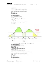
In order to ensure that also aquisition windows are aligned, it is necessary that also TRG-
IN is synchronised with EXT-CLK. Also edges must coincide in order to have alignment
between triggers and buffers.
3.2.10. Internal
clock
The board can work using the internal 50 MHz Local Oscillator as clock source. This
source is processed by the clock distribution electronics (AD9510 chip), which delivers
the 100 MHz Sampling Clock to the ADCs. The 100 MHz Sampling Clock is fed also to
the FPGA ROC (in order to allow trigger synchronisation, see also Fig. 1.1) and to
CLK_OUT (processed by a programmable divider and phase adjustment). Clock source
(internal or external) is selected via internal switch SW1 (see § 2.6).
3.2.11.
External clock and multiboard synchronisation
The board can work providing an external clock source (10÷100 MHz range). This source
is processed by the clock distribution electronics (AD9510 device), which delivers the 100
MHz Sampling Clock to the ADCs. The 100 MHz Sampling Clock is fed also to the FPGA
ROC (in order to allow trigger synchronisation) and to CLK_OUT (processed by a
programmable divider and phase adjustment). It is possible to adjust frequency and
phase of CLK_OUT and use such signal as clock source for another board, and so on, in
order to have the same clock source for all the boards.
Synchronisation is achieved, besides having the same clock source for all the boards,
with all the boards sharing the same trigger signal (TRG_IN), and a common
synchronisation (S_IN) signal: the latter is necessary in order to avoid a one Sampling
Clock period jitter.
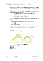
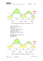
3.3. Acquisition
Modes
3.3.1. Acquisition
run/stop
The acquisition can be started in two ways, according to Acquisition Control register Bits
[1:0] setting (see § 4.17):
−
setting the RUN/STOP bit (bit[2]) in the Acquisition Control register (bits [1:0] of
Acquisition Control must be set to REGISTER-CONTROLLED RUN MODE
or S-IN
CONTROLLED RUN MODE)
−
driving S_IN signal high (bits [1:0] of Acquisition Control must be set to 01)


