
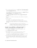


7.
Press
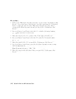
4
MKR
F
CTN
5
NNNNNNNNNNNNNNNNNNNNNNNNNNNNNNNNNNNNNNNNNNNNNNNNNN
MARKER
MODE
MENU
NNNNNNNNNNNNNNNNNNNNNNNNNN
STATS
ON
4
MENU
5
NNNNNNNNNNNNNNNNNNNNNNNNNNNNNNNNNNNNNN
TRIGGER
MENU
NNNNNNNNNNNNNNNNNNNNNNNNNNNNNNNNNNNNNNNNNNNNNNNNNN
NUMBER
of
GROUPS
4
5
5
4
x1
5 .
8.
When
the
trace
is
settled,
record
its
mean
value
(as
shown
on
the
analyzer's
display).
9.
Use
the
equation:
P
ower
(dBm)
=
20
*
f log
10
(linear
magnitude
mean
value)g
to
convert
the
linear
magnitude
mean
value
(measured
in
step
8)
to
log
magnitude
.
Record
this
calculated
value
on
the
\P
erformance
T
est
Record
(23
of
28)."
Note
If
your
analyzer
has
Option
003,
then
record
the
value
found
in
step
9
on
the
\P
erformance
T
est
Record
(23
of
28)"
under
section
HP
8752C
Options
075
and
003
ONL
Y
.
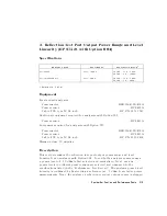
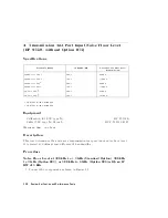
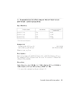
Noise
Floor
Level
at
300
kHz
to
1.3
GHz
(Option
075)
or
300
kHz
to
3
GHz
(Options
075
and
003)
with
an
IF
B
W
of
10
Hz
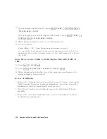
10.
Press
4
A
VG
5
NNNNNNNNNNNNNNNNN
IF
BW
4
1
5
4
0
5
4
x1
5
to
change
the
IF
bandwidth
to
10
Hz.
11.
Press
4
MENU
5
NNNNNNNNNNNNNNNNNNNNNNNNNNNNNNNNNNNNNN
TRIGGER
MENU
NNNNNNNNNNNNNNNNNNNN
SINGLE
.
12.
When
the
sweep
is
done
,
record
its
mean
value
.
Use
the
equation:
P
ower
(dBm)
=
20
*
f log10
(linear
magnitude
mean
value)g
to
convert
the
linear
magnitude
mean
value
to
log
magnitude
.
Record
this
calculated
value
on
the
\P
erformance
T
est
Record
(23
of
28)."
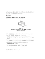
In
case
of
diculty
1.
Refer
to
the
\A
djustments
and
Correction
Constants"
chapter
.
P
erform
the
\ADC
Linearity
Correction
Constants
A
djustment"
procedure
.
Rerun
the
Transmission
T
est
P
ort
Input
Noise
Floor
Level
test.
2.
If
this
test
still
fails
,
suspect
the
A10
Digital
IF
board
assembly
.
3.
Refer
to
the
\Receiver
Troubleshooting"
section
in
this
manual
for
more
troubleshooting
information.
System
V
erication
and
P
erformance
T
ests
2-31
Содержание 8752C
Страница 22: ...Before Applying Power 15 6 Servicing 15 6 Index Contents 16 ...
Страница 38: ......
Страница 43: ...Figure 2 1 Measurement Uncertainty Window System Veri cation and Performance Tests 2 5 ...
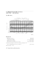
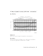
Страница 80: ...Figure 2 15 Magnitude Dynamic Accuracy Test Setup 2 42 System Veri cation and Performance Tests ...
Страница 116: ......
Страница 122: ...Figure 3 1 Location of Major Assemblies 3 6 Adjustments and Correction Constants ...
Страница 176: ......
Страница 192: ...4 16 Start Troubleshooting Here ...
Страница 193: ......
Страница 194: ...Figure 4 7 HP 8752C Overall Block Diagram 2 of 4 Option 003 and 004 Start Troubleshooting Here 4 19 ...
Страница 195: ...Figure 4 7 HP 8752C Overall Block Diagram 3 of 4 Option 006 4 20 Start Troubleshooting Here ...
Страница 196: ...Figure 4 7 HP 8752C Overall Block Diagram 4 of 4 Option 004 and 006 Start Troubleshooting Here 4 21 ...
Страница 197: ......
Страница 221: ...5 24 Power Supply Troubleshooting ...
Страница 222: ......
Страница 225: ...Digital Control Group Block Diagram Figure 6 1 Digital Control Group Block Diagram Digital Control Troubleshooting 6 3 ...
Страница 267: ...Figure 7 18 25 MHz HI OUT Waveform from A14J1 Figure 7 19 60 MHz HI OUT Waveform from A14J1 Source Troubleshooting 7 27 ...
Страница 271: ...Figure 7 21 A14 Generated Digital Control Signals Source Troubleshooting 7 31 ...
Страница 301: ...Figure 9 2 Typical Smith Chart Traces of Good Short a and Open b Accessories Troubleshooting 9 7 ...
Страница 302: ......
Страница 366: ......
Страница 378: ...Figure 11 4 Typical ED Re ection Test Port 11 12 Error Terms ...
Страница 380: ...Figure 11 5 Typical ES Re ection Test Port 11 14 Error Terms ...
Страница 382: ...Figure 11 6 Typical ER Re ection Test Port 11 16 Error Terms ...
Страница 384: ...Figure 11 7 Typical EX with 10 Hz Bandwidth Figure 11 8 Typical EX with 3 kHz Bandwidth 11 18 Error Terms ...
Страница 386: ...Figure 11 9 Typical ET 11 20 Error Terms ...
Страница 407: ...Figure 12 5 High Band Operation of the Source Theory of Operation 12 21 ...
Страница 410: ...Figure 12 6 Receiver Functional Group standard and Option 003 12 24 Theory of Operation ...
Страница 411: ...Figure 12 7 Receiver Functional Group Option 003 and 004 Theory of Operation 12 25 ...
Страница 412: ...Figure 12 8 Receiver Functional Group Option 006 12 26 Theory of Operation ...
Страница 413: ...Figure 12 9 Receiver Functional Group Option 004 and 006 Theory of Operation 12 27 ...
Страница 416: ......
Страница 419: ...Figure 13 1 Module Exchange Procedure Replaceable Parts 13 3 ...
Страница 423: ...Major Assemblies Replaceable Parts 13 7 ...
Страница 425: ...Front Panel Assemblies Replaceable Parts 13 9 ...
Страница 427: ...Rear Panel Assemblies Replaceable Parts 13 11 ...
Страница 429: ...Cables Top View Replaceable Parts 13 13 ...
Страница 431: ...Front Panel Cables and Attaching Hardware Replaceable Parts 13 15 ...
Страница 433: ...Rear Panel Cables and Attaching Hardware Replaceable Parts 13 17 ...
Страница 435: ...Source and Sampler Parts Standard and Option 003 Replaceable Parts 13 19 ...
Страница 437: ...Source and Sampler Parts Option 004 006 Replaceable Parts 13 21 ...
Страница 439: ...Source and Sampler Parts Options 004 and 003 004 Replaceable Parts 13 23 ...
Страница 441: ...Source and Sampler Parts Option 006 Replaceable Parts 13 25 ...
Страница 443: ...Display Bezel Assembly Replaceable Parts 13 27 ...
Страница 445: ...Chassis Parts Replaceable Parts 13 29 ...
Страница 447: ...Top View of Attaching Hardware and Post Regulator Fuses Replaceable Parts 13 31 ...
Страница 449: ...Bottom View of Attaching Hardware Replaceable Parts 13 33 ...
Страница 488: ......