
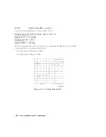


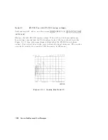

Node
11
A
ux
Input
(rear
panel
input)
P
erform
step
A10,
above
,
and
then
press
4
MEAS
5
N
NNNNNNNNNNNNNNNNNNNNNNNNNNNN
ANALOG
IN
4
1
5
4
1
5
4
x1
5 .
This
selects
the
rear
panel
A
UX
INPUT
to
drive
the
analog
bus
for
voltage
and
frequency
measurements
.
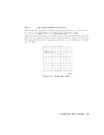
It
can
be
used
to
look
at
test
points
within
the
instrument,
using
the
analyzer's
display
as
an
oscilloscope
.
Connect
the
test
point
of
interest
to
the
rear
panel
A
UX
INPUT
BNC
connector
.
This
feature
can
be
useful
if
an
oscilloscope
is
not
available
.
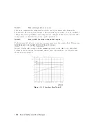
Also
,
it
can
be
used
for
testing
voltage-controlled
devices
by
connecting
the
driving
voltage
of
the
device
under
test
to
the
A
UX
IN
connector
.
Look
at
the
driving
voltage
on
one
display
channel,
while
displaying
the
S-parameter
response
of
the
test
device
on
the
other
display
channel.
With
NNNNNNNNNNNNNNNNNNNNNNN
AUX
OUT
switched
ON,
you
can
examine
the
analyzer's
analog
bus
nodes
with
external
equipment
(see
NNNNNNNNNNNNNNNNNNNNNNNNNNNNNNNNNNNNNNNNNNNN
AUX
OUT
on
OFF
under
the
\Analog
Bus
Menu"
heading).
F
or
HP-IB
considerations
,
see
\HP-IB
Service
Mnemonic
Denitions
,"
located
later
in
this
chapter
.
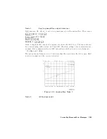
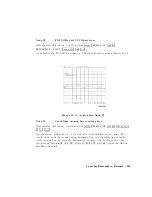
Node
12
A10
Gnd
(ground
reference)
This
node
is
used
in
the
\Analog
Bus
Correction
Constants"
adjustment
as
a
reference
for
calibrating
the
analog
bus
low
and
high
resolution
circuitry
.
A11
Phase
Lock
T
o
observe
the
A11
analog
bus
nodes
perform
step
A11,
below
.
Then
follow
the
node-specic
instructions
.
Step
A11.
Press:
4
PRESET
5
4
MEAS
5
NNNNNNNNNNNNNNNNNNNNNNNNNNNNN
ANALOG
IN
4
MKR
5
4
SYSTEM
5
NNNNNNNNNNNNNNNNNNNNNNNNNNNNNNNNNNNNNN
SERVICE
MENU
NNNNNNNNNNNNNNNNNNNNNNNNNNNNNNNNNNNNNNNNN
ANALOG
BUS
ON
Node
13
V
CO
Tune
2
(not
used)
Service
K
ey
Menus
and
Error
Messages
10-37
Содержание 8752C
Страница 22: ...Before Applying Power 15 6 Servicing 15 6 Index Contents 16 ...
Страница 38: ......
Страница 43: ...Figure 2 1 Measurement Uncertainty Window System Veri cation and Performance Tests 2 5 ...
Страница 80: ...Figure 2 15 Magnitude Dynamic Accuracy Test Setup 2 42 System Veri cation and Performance Tests ...
Страница 116: ......
Страница 122: ...Figure 3 1 Location of Major Assemblies 3 6 Adjustments and Correction Constants ...
Страница 176: ......
Страница 192: ...4 16 Start Troubleshooting Here ...
Страница 193: ......
Страница 194: ...Figure 4 7 HP 8752C Overall Block Diagram 2 of 4 Option 003 and 004 Start Troubleshooting Here 4 19 ...
Страница 195: ...Figure 4 7 HP 8752C Overall Block Diagram 3 of 4 Option 006 4 20 Start Troubleshooting Here ...
Страница 196: ...Figure 4 7 HP 8752C Overall Block Diagram 4 of 4 Option 004 and 006 Start Troubleshooting Here 4 21 ...
Страница 197: ......
Страница 221: ...5 24 Power Supply Troubleshooting ...
Страница 222: ......
Страница 225: ...Digital Control Group Block Diagram Figure 6 1 Digital Control Group Block Diagram Digital Control Troubleshooting 6 3 ...
Страница 267: ...Figure 7 18 25 MHz HI OUT Waveform from A14J1 Figure 7 19 60 MHz HI OUT Waveform from A14J1 Source Troubleshooting 7 27 ...
Страница 271: ...Figure 7 21 A14 Generated Digital Control Signals Source Troubleshooting 7 31 ...
Страница 301: ...Figure 9 2 Typical Smith Chart Traces of Good Short a and Open b Accessories Troubleshooting 9 7 ...
Страница 302: ......
Страница 366: ......
Страница 378: ...Figure 11 4 Typical ED Re ection Test Port 11 12 Error Terms ...
Страница 380: ...Figure 11 5 Typical ES Re ection Test Port 11 14 Error Terms ...
Страница 382: ...Figure 11 6 Typical ER Re ection Test Port 11 16 Error Terms ...
Страница 384: ...Figure 11 7 Typical EX with 10 Hz Bandwidth Figure 11 8 Typical EX with 3 kHz Bandwidth 11 18 Error Terms ...
Страница 386: ...Figure 11 9 Typical ET 11 20 Error Terms ...
Страница 407: ...Figure 12 5 High Band Operation of the Source Theory of Operation 12 21 ...
Страница 410: ...Figure 12 6 Receiver Functional Group standard and Option 003 12 24 Theory of Operation ...
Страница 411: ...Figure 12 7 Receiver Functional Group Option 003 and 004 Theory of Operation 12 25 ...
Страница 412: ...Figure 12 8 Receiver Functional Group Option 006 12 26 Theory of Operation ...
Страница 413: ...Figure 12 9 Receiver Functional Group Option 004 and 006 Theory of Operation 12 27 ...
Страница 416: ......
Страница 419: ...Figure 13 1 Module Exchange Procedure Replaceable Parts 13 3 ...
Страница 423: ...Major Assemblies Replaceable Parts 13 7 ...
Страница 425: ...Front Panel Assemblies Replaceable Parts 13 9 ...
Страница 427: ...Rear Panel Assemblies Replaceable Parts 13 11 ...
Страница 429: ...Cables Top View Replaceable Parts 13 13 ...
Страница 431: ...Front Panel Cables and Attaching Hardware Replaceable Parts 13 15 ...
Страница 433: ...Rear Panel Cables and Attaching Hardware Replaceable Parts 13 17 ...
Страница 435: ...Source and Sampler Parts Standard and Option 003 Replaceable Parts 13 19 ...
Страница 437: ...Source and Sampler Parts Option 004 006 Replaceable Parts 13 21 ...
Страница 439: ...Source and Sampler Parts Options 004 and 003 004 Replaceable Parts 13 23 ...
Страница 441: ...Source and Sampler Parts Option 006 Replaceable Parts 13 25 ...
Страница 443: ...Display Bezel Assembly Replaceable Parts 13 27 ...
Страница 445: ...Chassis Parts Replaceable Parts 13 29 ...
Страница 447: ...Top View of Attaching Hardware and Post Regulator Fuses Replaceable Parts 13 31 ...
Страница 449: ...Bottom View of Attaching Hardware Replaceable Parts 13 33 ...
Страница 488: ......