


If
the
Green
LEDs
On
A8
are
not
All
On
The
green
LEDs
along
the
top
edge
of
the
A8
post
regulator
are
normally
on.
Flashing
LEDs
on
A8
indicate
that
the
shutdown
circuitry
on
the
A8
post
regulator
is
protecting
power
supplies
from
overcurrent
conditions
by
repeatedly
shutting
them
down.
This
may
be
caused
by
supply
loading
on
A8
or
on
any
other
assembly
in
the
analyzer
.
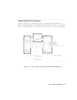
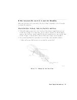
Remove
A8,
Maintain
A15W1
Cable
Connection
1.
Switch
o
the
analyzer
.
2.
Remove
A8
from
its
motherboard
connector
,
but
keep
the
A15W1
cable
connected
to
A8.
3.
Remove
the
display
power
cable
W14
(see
Figure
5-5).
4.
Short
A8TP2
(A
GND)
(see
Figure
5-3)
to
chassis
ground
with
a
clip
lead.
5.
Switch
on
the
analyzer
and
observe
the
green
LEDs
on
A8.
If
any
green
LEDs
other
than
+5VD
are
still
o
or
ashing,
continue
with
\Check
the
A8
Fuses
and
V
oltages
."
If
all
LEDs
are
now
on
steadily
except
for
the
+5VD
LED
,
the
A15
preregulator
and
A8
post
regulator
are
working
properly
and
the
trouble
is
excessive
loading
somewhere
after
the
motherboard
connections
at
A8.
Continue
with
\Remove
the
Assemblies
."
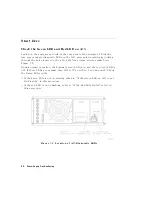
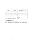
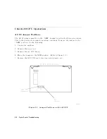
Check
the
A8
Fuses
and
V
oltages
Check
the
fuses
along
the
top
edge
of
A8.
If
any
A8
fuse
has
burned
out,
replace
it.
If
it
burns
out
again
when
power
is
applied
to
the
analyzer
,
A8
or
A15
is
faulty
.
Determine
which
assembly
has
failed
as
follows
.
1.
Remove
the
A15W1
cable
at
A8
(see
Figure
5-5).
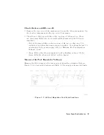
2.
Measure
the
voltages
at
A15W1P1
(see
Figure
5-6)
with
a
voltmeter
that
has
a
small
probe
.
3.
Compare
the
measured
voltages
with
those
in
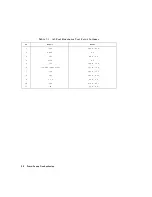
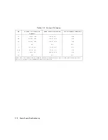
T
able
5-2 .
If
the
voltages
are
within
tolerance
,
replace
A8.
If
the
voltages
are
not
within
tolerance
,
replace
A15.
5-14
P
ower
Supply
T
roubleshooting
Содержание 8752C
Страница 22: ...Before Applying Power 15 6 Servicing 15 6 Index Contents 16 ...
Страница 38: ......
Страница 43: ...Figure 2 1 Measurement Uncertainty Window System Veri cation and Performance Tests 2 5 ...
Страница 80: ...Figure 2 15 Magnitude Dynamic Accuracy Test Setup 2 42 System Veri cation and Performance Tests ...
Страница 116: ......
Страница 122: ...Figure 3 1 Location of Major Assemblies 3 6 Adjustments and Correction Constants ...
Страница 176: ......
Страница 192: ...4 16 Start Troubleshooting Here ...
Страница 193: ......
Страница 194: ...Figure 4 7 HP 8752C Overall Block Diagram 2 of 4 Option 003 and 004 Start Troubleshooting Here 4 19 ...
Страница 195: ...Figure 4 7 HP 8752C Overall Block Diagram 3 of 4 Option 006 4 20 Start Troubleshooting Here ...
Страница 196: ...Figure 4 7 HP 8752C Overall Block Diagram 4 of 4 Option 004 and 006 Start Troubleshooting Here 4 21 ...
Страница 197: ......
Страница 221: ...5 24 Power Supply Troubleshooting ...
Страница 222: ......
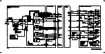
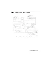
Страница 225: ...Digital Control Group Block Diagram Figure 6 1 Digital Control Group Block Diagram Digital Control Troubleshooting 6 3 ...
Страница 267: ...Figure 7 18 25 MHz HI OUT Waveform from A14J1 Figure 7 19 60 MHz HI OUT Waveform from A14J1 Source Troubleshooting 7 27 ...
Страница 271: ...Figure 7 21 A14 Generated Digital Control Signals Source Troubleshooting 7 31 ...
Страница 301: ...Figure 9 2 Typical Smith Chart Traces of Good Short a and Open b Accessories Troubleshooting 9 7 ...
Страница 302: ......
Страница 366: ......
Страница 378: ...Figure 11 4 Typical ED Re ection Test Port 11 12 Error Terms ...
Страница 380: ...Figure 11 5 Typical ES Re ection Test Port 11 14 Error Terms ...
Страница 382: ...Figure 11 6 Typical ER Re ection Test Port 11 16 Error Terms ...
Страница 384: ...Figure 11 7 Typical EX with 10 Hz Bandwidth Figure 11 8 Typical EX with 3 kHz Bandwidth 11 18 Error Terms ...
Страница 386: ...Figure 11 9 Typical ET 11 20 Error Terms ...
Страница 407: ...Figure 12 5 High Band Operation of the Source Theory of Operation 12 21 ...
Страница 410: ...Figure 12 6 Receiver Functional Group standard and Option 003 12 24 Theory of Operation ...
Страница 411: ...Figure 12 7 Receiver Functional Group Option 003 and 004 Theory of Operation 12 25 ...
Страница 412: ...Figure 12 8 Receiver Functional Group Option 006 12 26 Theory of Operation ...
Страница 413: ...Figure 12 9 Receiver Functional Group Option 004 and 006 Theory of Operation 12 27 ...
Страница 416: ......
Страница 419: ...Figure 13 1 Module Exchange Procedure Replaceable Parts 13 3 ...
Страница 423: ...Major Assemblies Replaceable Parts 13 7 ...
Страница 425: ...Front Panel Assemblies Replaceable Parts 13 9 ...
Страница 427: ...Rear Panel Assemblies Replaceable Parts 13 11 ...
Страница 429: ...Cables Top View Replaceable Parts 13 13 ...
Страница 431: ...Front Panel Cables and Attaching Hardware Replaceable Parts 13 15 ...
Страница 433: ...Rear Panel Cables and Attaching Hardware Replaceable Parts 13 17 ...
Страница 435: ...Source and Sampler Parts Standard and Option 003 Replaceable Parts 13 19 ...
Страница 437: ...Source and Sampler Parts Option 004 006 Replaceable Parts 13 21 ...
Страница 439: ...Source and Sampler Parts Options 004 and 003 004 Replaceable Parts 13 23 ...
Страница 441: ...Source and Sampler Parts Option 006 Replaceable Parts 13 25 ...
Страница 443: ...Display Bezel Assembly Replaceable Parts 13 27 ...
Страница 445: ...Chassis Parts Replaceable Parts 13 29 ...
Страница 447: ...Top View of Attaching Hardware and Post Regulator Fuses Replaceable Parts 13 31 ...
Страница 449: ...Bottom View of Attaching Hardware Replaceable Parts 13 33 ...
Страница 488: ......