


Check
Input
Trace
All
inputs
to
the
sampler
have
been
veried
except
for
the
signal
coming
from
the
coupler
.
The
problem
is
most
likely
a
faulty
coupler
or
sampler
.
However
,
the
A10
assembly
may
also
be
at
fault.
Press
4
PRESET
5
4
MEAS
5
NNNNNNNNNNNNNNNNNNNNNNNNNNNNNNNNNNN
INPUT
PORTS
and
select
the
input
with
the
bad
trace
.
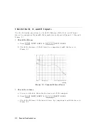
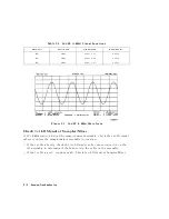
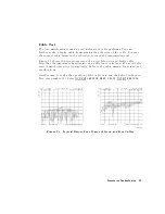
The
trace
normally
has
a
number
of
jumps
in
it
due
to
band
switches
,
as
shown
in
Figure
8-1
through
Figure
8-3.
Each
jump
should
be
less
than
2
dB
.
If
there
are
other
peaks
or
holes
in
the
trace
,
the
sampler
is
probably
faulty
.
Remove
the
suspected
sampler
and
exchange
it
with
the
known
good
sampler
.
If
the
problem
disappears
,
replace
the
suspected
sampler
.
If
there
is
a
broadband
problem,
it
is
probably
caused
by
the
coupler
.
If
the
level
(average
value)
of
the
trace
is
wrong
but
the
trace
is
otherwise
correct,
the
problem
is
most
likely
in
the
coupler
or
the
A10
assembly
.
Either
measure
the
output
of
the
coupler
with
a
power
meter
,
or
swap
the
A10
assembly
with
another
known
working
A10
assembly
.
Check
directivity
,
source
match,
and
crosstalk
by
performing
the
system
verication
procedure
described
in
the
\System
V
erication
and
P
erformance
T
ests"
chapter
.
If
any
of
these
fail,
check
the
coupler
and
sampler
connections
.
T
o
verify
the
coupler
is
faulty
,
remove
the
sampler
that
has
the
bad
input
and
exchange
it
with
the
known
good
sampler
.
If
there
is
no
improvement,
replace
the
coupler
.
If
the
problem
disappears
,
replace
the
original
sampler
.
If
the
2nd
LO
is
good
at
the
sampler/mixer
,
the
sampler/mixer
assembly
is
faulty
.
Otherwise
,
troubleshoot
the
A12
assembly
and
associated
signal
path.
8-14
Receiver
T
roubleshooting
Содержание 8752C
Страница 22: ...Before Applying Power 15 6 Servicing 15 6 Index Contents 16 ...
Страница 38: ......
Страница 43: ...Figure 2 1 Measurement Uncertainty Window System Veri cation and Performance Tests 2 5 ...
Страница 80: ...Figure 2 15 Magnitude Dynamic Accuracy Test Setup 2 42 System Veri cation and Performance Tests ...
Страница 116: ......
Страница 122: ...Figure 3 1 Location of Major Assemblies 3 6 Adjustments and Correction Constants ...
Страница 176: ......
Страница 192: ...4 16 Start Troubleshooting Here ...
Страница 193: ......
Страница 194: ...Figure 4 7 HP 8752C Overall Block Diagram 2 of 4 Option 003 and 004 Start Troubleshooting Here 4 19 ...
Страница 195: ...Figure 4 7 HP 8752C Overall Block Diagram 3 of 4 Option 006 4 20 Start Troubleshooting Here ...
Страница 196: ...Figure 4 7 HP 8752C Overall Block Diagram 4 of 4 Option 004 and 006 Start Troubleshooting Here 4 21 ...
Страница 197: ......
Страница 221: ...5 24 Power Supply Troubleshooting ...
Страница 222: ......
Страница 225: ...Digital Control Group Block Diagram Figure 6 1 Digital Control Group Block Diagram Digital Control Troubleshooting 6 3 ...
Страница 267: ...Figure 7 18 25 MHz HI OUT Waveform from A14J1 Figure 7 19 60 MHz HI OUT Waveform from A14J1 Source Troubleshooting 7 27 ...
Страница 271: ...Figure 7 21 A14 Generated Digital Control Signals Source Troubleshooting 7 31 ...
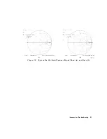
Страница 301: ...Figure 9 2 Typical Smith Chart Traces of Good Short a and Open b Accessories Troubleshooting 9 7 ...
Страница 302: ......
Страница 366: ......
Страница 378: ...Figure 11 4 Typical ED Re ection Test Port 11 12 Error Terms ...
Страница 380: ...Figure 11 5 Typical ES Re ection Test Port 11 14 Error Terms ...
Страница 382: ...Figure 11 6 Typical ER Re ection Test Port 11 16 Error Terms ...
Страница 384: ...Figure 11 7 Typical EX with 10 Hz Bandwidth Figure 11 8 Typical EX with 3 kHz Bandwidth 11 18 Error Terms ...
Страница 386: ...Figure 11 9 Typical ET 11 20 Error Terms ...
Страница 407: ...Figure 12 5 High Band Operation of the Source Theory of Operation 12 21 ...
Страница 410: ...Figure 12 6 Receiver Functional Group standard and Option 003 12 24 Theory of Operation ...
Страница 411: ...Figure 12 7 Receiver Functional Group Option 003 and 004 Theory of Operation 12 25 ...
Страница 412: ...Figure 12 8 Receiver Functional Group Option 006 12 26 Theory of Operation ...
Страница 413: ...Figure 12 9 Receiver Functional Group Option 004 and 006 Theory of Operation 12 27 ...
Страница 416: ......
Страница 419: ...Figure 13 1 Module Exchange Procedure Replaceable Parts 13 3 ...
Страница 423: ...Major Assemblies Replaceable Parts 13 7 ...
Страница 425: ...Front Panel Assemblies Replaceable Parts 13 9 ...
Страница 427: ...Rear Panel Assemblies Replaceable Parts 13 11 ...
Страница 429: ...Cables Top View Replaceable Parts 13 13 ...
Страница 431: ...Front Panel Cables and Attaching Hardware Replaceable Parts 13 15 ...
Страница 433: ...Rear Panel Cables and Attaching Hardware Replaceable Parts 13 17 ...
Страница 435: ...Source and Sampler Parts Standard and Option 003 Replaceable Parts 13 19 ...
Страница 437: ...Source and Sampler Parts Option 004 006 Replaceable Parts 13 21 ...
Страница 439: ...Source and Sampler Parts Options 004 and 003 004 Replaceable Parts 13 23 ...
Страница 441: ...Source and Sampler Parts Option 006 Replaceable Parts 13 25 ...
Страница 443: ...Display Bezel Assembly Replaceable Parts 13 27 ...
Страница 445: ...Chassis Parts Replaceable Parts 13 29 ...
Страница 447: ...Top View of Attaching Hardware and Post Regulator Fuses Replaceable Parts 13 31 ...
Страница 449: ...Bottom View of Attaching Hardware Replaceable Parts 13 33 ...
Страница 488: ......